The ccs is not secret, its been used by others too, I didnt design it, baxandall did, its open source. Watch carefull for oscilation but if correctly used its just dandy
Os the changes I recommend is as I stated in that post try it, just change those resistor values and watch the drop in THD and also noise. The harmonic spectrum stays the exact same only at much lower level. I use the mongrel sim fet amp file, change to 2sk170 jfets, change r11 and r12 to 10 ohms, than up current of ccs and get at least 2ma across each jfet, more is better but then you might have to change compensation, then watch the drop in THD. The amp is then basically a replica of a amp I have used many years and still do except I use toshiba mosfets as outputs in a triple configuration.
What is handy is that one can use the same pcb as the BJT model, just change those few components and have a good jfet input amp with the advantages it represents. You can drop the feedback cap and use much lower feedback resistor value and drop the noise of the amp substancially.
Last edited:
#1-The ccs is not secret, its been used by others too, I didnt design it, baxandall did, its open source. Watch carefull for oscillation.
#2- What is handy is that one can use the same pcb as the BJT model, just change those few components and have a good jfet input amp with the advantages it represents.
1-Under what conditions is there oscillation ?
2- So you say the 170 's will drop right in (D-G-S ?).
Another reason I haven't used the FET's is that $$$ they are expensive!!
OS
1 If youre lucky you wont have any problem with the ccs, try it, I never figured out under what conditions, some times it gets the whole amp unstable, the one South African member experimented quite a bit with it but I cant recall his name now, using it with a complementary ltp input amp he got very good results.
2. I dont know, I havent looked at the layout of that amp, but it s no big feat bending a leg or 2. 2sk170 Jfets can be purchased for 50c each, matched ones at 1,50 dollars, I dont think this is expensive, I would rather use bf862 jfets anyway and just solder them on a little adapter first, these jfets cost 15c and offer better performance than the toshibas. In my amps Im using 2sk223 which I purchased in bulk for just over 8c each but when they finish as they are discontinued Ill be changing to the bf862 and design a little adapter for them.
2. I dont know, I havent looked at the layout of that amp, but it s no big feat bending a leg or 2. 2sk170 Jfets can be purchased for 50c each, matched ones at 1,50 dollars, I dont think this is expensive, I would rather use bf862 jfets anyway and just solder them on a little adapter first, these jfets cost 15c and offer better performance than the toshibas. In my amps Im using 2sk223 which I purchased in bulk for just over 8c each but when they finish as they are discontinued Ill be changing to the bf862 and design a little adapter for them.
Last edited:
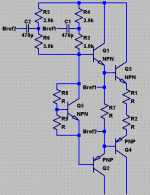
Alright then Homemodder, I'll open up for Exhibit A: a really good CCS.
Attached is a schematic of the Baxandall CCS. To my knowledge the 3rd transistor came afterwards, but whatever. It works too well to keep under wraps. The 100p cap helps oscillation in simulation.
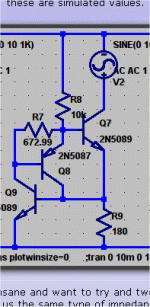
The second version shows a "Tweaked" version. The funny thing about this CCS is that it actually uses positive feedback, and so the output is actually overcompensated - it is a negative impedance CCS. If we tweak it so that very little current flows through the PNP, we decrease the positive feedback and eventually find the place where phase turns back 90 degrees - perfectly compensated. Unfortunately in doing this the BW is lost over the two-Q CCS, and there is also a bottom limit because of temperature drift.
In the common two-transistor CCS, shown 3rd, Early affect causes Ib to change with Vce, causing error. The greater the Hfe of the output transistor, the better. But if a low-Hfe several watt type is used for a power amp, the setback can be severe. The devastating effects of Early affect are even worse for the two-diode version 5. Here, the OPT's Vbe changes with Vce, terribly affecting output current.
The funny thing is that these distortions make a CCS worse in some applications than a simple bootstrap. CCS's create high order distortions especially when nearing saturation. Resistors create no such distortions, and are trivial. In many cases, bootstraps can be more effective than a CCS at audio frequencies. I have attached my preferred current source last... BW is no issue here. We do not worry about loading the VAS excessively as is usually the worry with referencing bootstrap directly to the output. It cannot create the higher order distortions of a semiconductor CCS.
The Baxandall CCS as shown circuits 1 and 2 from left, gets around the Ib problem by rerouting all Ib to the current sense resistor, so it is not missing from the feedback loop. Vbe of the OPT is negligible just as in the 3rd circuit, because of the feedback loop.
What's more HF impedance is greatly increased, because of the same mechanism by which Ib is rerouted to the current sense. Signals coming from Cob are rerouted from the base of the OPT to it's emitter where the loop cancels itself out. If careful, this allows for a steady -150db impedance across the audio band. That's 30 megaohms.
1st circuit: 30 megaohms .1pF
2nd circuit: 22 megaohms at 10KHz, 6db/octave. Lower limit ~165db or 196meg with +-5C .86pF
3rd circuit: 13 megaohms 2pF
4th circuit: 297kohms 3pF
Disclaimer: these are simulated values.
- keantoken
Attached is a schematic of the Baxandall CCS. To my knowledge the 3rd transistor came afterwards, but whatever. It works too well to keep under wraps. The 100p cap helps oscillation in simulation.
The second version shows a "Tweaked" version. The funny thing about this CCS is that it actually uses positive feedback, and so the output is actually overcompensated - it is a negative impedance CCS. If we tweak it so that very little current flows through the PNP, we decrease the positive feedback and eventually find the place where phase turns back 90 degrees - perfectly compensated. Unfortunately in doing this the BW is lost over the two-Q CCS, and there is also a bottom limit because of temperature drift.
In the common two-transistor CCS, shown 3rd, Early affect causes Ib to change with Vce, causing error. The greater the Hfe of the output transistor, the better. But if a low-Hfe several watt type is used for a power amp, the setback can be severe. The devastating effects of Early affect are even worse for the two-diode version 5. Here, the OPT's Vbe changes with Vce, terribly affecting output current.
The funny thing is that these distortions make a CCS worse in some applications than a simple bootstrap. CCS's create high order distortions especially when nearing saturation. Resistors create no such distortions, and are trivial. In many cases, bootstraps can be more effective than a CCS at audio frequencies. I have attached my preferred current source last... BW is no issue here. We do not worry about loading the VAS excessively as is usually the worry with referencing bootstrap directly to the output. It cannot create the higher order distortions of a semiconductor CCS.
The Baxandall CCS as shown circuits 1 and 2 from left, gets around the Ib problem by rerouting all Ib to the current sense resistor, so it is not missing from the feedback loop. Vbe of the OPT is negligible just as in the 3rd circuit, because of the feedback loop.
What's more HF impedance is greatly increased, because of the same mechanism by which Ib is rerouted to the current sense. Signals coming from Cob are rerouted from the base of the OPT to it's emitter where the loop cancels itself out. If careful, this allows for a steady -150db impedance across the audio band. That's 30 megaohms.
1st circuit: 30 megaohms .1pF
2nd circuit: 22 megaohms at 10KHz, 6db/octave. Lower limit ~165db or 196meg with +-5C .86pF
3rd circuit: 13 megaohms 2pF
4th circuit: 297kohms 3pF
Disclaimer: these are simulated values.
- keantoken
Attachments
If you're insane and want to try and tweak it, I've discovered a better way decrease positive feedback is to put a ~180 ohm resistor at Q3's emitter. This gives us the same type of impedance as the second circuit, but a lower bottom limit and better BW at 20G+.1pF +-5C if simulation can be trusted. However this increases sensitivity to ripple entering through R1. I don't think this is an issue if you filter your frontend rails.
- keantoken
- keantoken
Last edited:
If you're insane and want to try and tweak it, I've discovered a better way decrease positive feedback is to put a ~180 ohm resistor at Q3's emitter. This gives us the same type of impedance as the second circuit, but a lower bottom limit and better BW at 20G+.1pF +-5C if simulation can be trusted. However this increases sensitivity to ripple entering through R1. I don't think this is an issue if you filter your frontend rails.
- keantoken
I AM insane..
 First, I like the 2nd CCS (below). Also, is that last shot of a type 2 EF with dual bootstraps taken from either side of of the driver emitter resistor ?? Have you simmed a whole amp with a setup like this ?
OS
Attachments
Intersting thread. I did some simulations BTW on active CCS as above and also on using a zener and a resistor to derive the CC. I think the CCS performance over frequency is more important than the absolute output impeadance. Zener resistor combo is surprisingly good, showing best wide band performance.
The ccs is not secret, its been used by others too, I didnt design it, baxandall did, its open source. Watch carefull for oscilation but if correctly used its just dandy
Os the changes I recommend is as I stated in that post try it, just change those resistor values and watch the drop in THD and also noise. The harmonic spectrum stays the exact same only at much lower level. I use the mongrel sim fet amp file, change to 2sk170 jfets, change r11 and r12 to 10 ohms, than up current of ccs and get at least 2ma across each jfet, more is better but then you might have to change compensation, then watch the drop in THD. The amp is then basically a replica of a amp I have used many years and still do except I use toshiba mosfets as outputs in a triple configuration.
What is handy is that one can use the same pcb as the BJT model, just change those few components and have a good jfet input amp with the advantages it represents. You can drop the feedback cap and use much lower feedback resistor value and drop the noise of the amp substancially.
Re the suggestion to use JFET's: I know this amp is capacitively coupled, but even after zeroing the output, are you not going to have temperature induced offset drift problems due to the JFET's? You might need some kind of servo to sort this out.
By Bonsai - Re the suggestion to use JFET's: I know this amp is capacitively coupled, but even after zeroing the output, are you not going to have temperature induced offset drift problems due to the JFET's? You might need some kind of servo to sort this out.
look at the pioneer m-90 below, no servo! many other 80's amps use the JFETS also with no servo. They DO use a dual device.
OS
Attachments
I AM insane..
OS
I've never found the need to use the super-CCS, after several megaohms impedance it gets redundant... I rarely use LTP's either. I have never had a good reason to use a fancy CCS, except for test equipment, where they can be really handy. An interesting application is a sweep/pulse generator, I have one in simulation getting an 8nS pulse. Here the CCS MUST have fast recovery time, and MUST have good HF behavior, AS WELL as having extremely high impedance for an honest sweep. No digital here!
If you want, I could throw together an amp topology of your choice, and assess the benefit of different CCS configurations.
I did some simulations BTW on active CCS as above and also on using a zener and a resistor to derive the CC. I think the CCS performance over frequency is more important than the absolute output impeadance.
So you're saying that impedance doesn't matter so much as long as the corner frequency(s) are outside of the audio spectrum? For instance, a good CCS might give -150db with a corner of 20KHz, but increase the impedance to 180db without changing BW and now the corner frequency is in the middle of the audio spectrum. You would opt for the CCS with no phase or impedance anomalies in the audio spectrum, regardless of impedance?
- keantoken
I would rephrase that to one could opt for the CCS with no phase or impedance anomaly below 100kHz and controlled (damped) behaviour above that along with a reasonable CCS impedance to match it's duty............ would opt for the CCS with no phase or impedance anomalies in the audio spectrum, regardless of impedance?
Quote" So you're saying that impedance doesn't matter so much as long as the corner frequency(s) are outside of the audio spectrum? For instance, a good CCS might give -150db with a corner of 20KHz, but increase the impedance to 180db without changing BW and now the corner frequency is in the middle of the audio spectrum. You would opt for the CCS with no phase or impedance anomalies in the audio spectrum, regardless of impedance?"
If you look at a straight zener resistor combo vs an active 2 or 3 transistor circuit, the zener resistor combo is about 6-8 db worse than the active type at low frequencies, but beyond about 500Hz, its Zo is flat out to about 200KHz whereas the active types degenerate from about 1-2KHz. Both types are good, but the zener+resistor circuit is in my veiw remarkably good for how simple it is.
If you look at a straight zener resistor combo vs an active 2 or 3 transistor circuit, the zener resistor combo is about 6-8 db worse than the active type at low frequencies, but beyond about 500Hz, its Zo is flat out to about 200KHz whereas the active types degenerate from about 1-2KHz. Both types are good, but the zener+resistor circuit is in my veiw remarkably good for how simple it is.
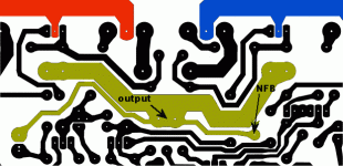
BTW, I looked at the PCB layout on the 250W version. I note that the feedback resistor take-off point is towards the first set of output emitter resistors. In line with Self's comments on this, it would be better to take th e feedback off from just before the output inductor. You may want to take a look at this.
BTW, I looked at the PCB layout on the 250W version. I note that the feedback resistor take-off point is towards the first set of output emitter resistors. In line with Self's comments on this, it would be better to take th e feedback off from just before the output inductor. You may want to take a look at this.
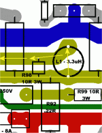
This is something I really did think about. In the normal DIYA layout (dx ,symasym ) the emitter resistors are at the sides (left and right) and the current pulses from the main OP's meet at the middle where the large traces meet (pix 1 - typical.gif). The Doug Self amp PCB is like this ,too.
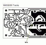
In the quasi NMOS 350 (pix2 -below) , Lynx ,PB250, any of the symmetric layouts, the pulses meet at the middle of the OP bus. You could scope the middle anywhere along the 175mm of the PB250 output bus and the signal should be EXACTLY the same from one end to the other .
I do see your point , Bonsai. Where the OP inductor's trace comes off is a right turn off the "FREEWAY" (OP BUS) , and might be different than what "you" as a scope or DMM might see standing in the middle of the "FREEWAY".
Another way to make the NFB signal match that of the inductor, is to have the inductor trace fed by a jumper coming from the MIDDLE of the "freeway" .
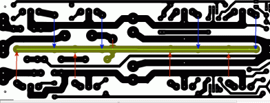
Look
 at pix 3 below to visualize what I say (yellow line is the "middle/center point" of trace , red/blue are currents from + / - OP's).
NFB takeoff between 2 emitter resistors at one end of rail should be the EXACT same signal as between opposing emitter resistors at the other end of the bus.
OS
Attachments
Last edited:
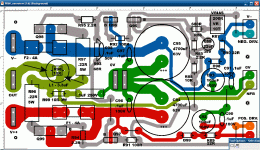
This would not of "broke the amp" BUT , as a perfectionist ... I changed it.
The "fix" (below)... I can take that criticism (In fact I welcome it ) ,and implement it. The inductor will be vertical instead of horizontal and will tap the middle of the "freeway"
..will update zipfile soon.
OS
The "fix" (below)... I can take that criticism (In fact I welcome it
) ,and implement it. The inductor will be vertical instead of horizontal and will tap the middle of the "freeway"..will update zipfile soon.
OS
Attachments
Looks good! What pcb package are you using BTW?
You would be SHOCKED ! NONE... actually "JASC paint shop pro 9" with custom pads (called "tubes") and mental layout. Layouts are 1200 DPI for absolute 600 DPI printer output.
I also fixed the PB60 with the same vertical inductor scheme. resistor is inside the inductor. The PB60 has only 2 Op devices making for a perfect "self" NFB takeoff. (pix below)
The layout here is one "cut above" the symasym , quasi ... fat pads to facilitate sloppy solderers as well.
the mouser FR-4 can also take almost unlimited 350c heat with no pad separation.. highly recommended .An externally hosted image should be here but it was not working when we last tested it.
Copper Clad Boards
OS
Attachments
Last edited:
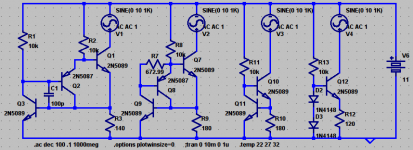
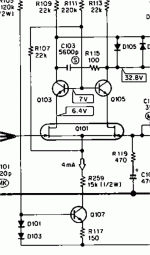
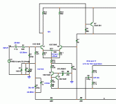
On with the BX1.1VB (Bootstrap amp). This was such a big surprise !!
First the schematic (pix 1).
You can see what I did... no biggie. WHY is the question ... as you can see the tail has both the original resistive current source and a CCS (horrid). The CCS is there to allow for both fine trimming (R6 - 200R/CCS ADJ.) of the tail currents and adjustment for the transition from "baby" (50w - PB60) to the "real deal" (250w - PB250). The only "hard" change required is R16-17 . This keeps the VAS @ 6.5 to 7 mA , which is required to allow for proper biasing on the 2 power boards.
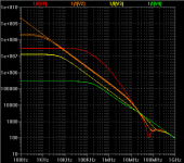
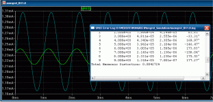
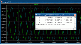
(pix 2) Shows THD @ 1khz / 50w , not bad for 5 parts. Balanced tails are even more important with this amp , unbalanced was .05% dropping to the shown .004% at the KSC's "sweet spot" (1.2mA)
(pix 3) Shows some "serious distortion" .018% ooohhhh .. (I am spoiled by the self amp - AX)
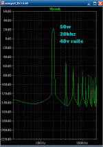
(Pix 4) This where I A/B'ed this creation against the "baseline" , which was the original "baby 55" (BC-xxx semi's and all original values @40v rails). The FFT's were similar if not exact @ 1k . At 20k , this amp beat the pants off of the "baby" .... lower THD as well as holding the same 1KhZ harmonic structure at this higher frequency.
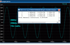
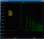
(Pix 5-6) This is where I had to see whether my little VB could take the "heat" .. 200w operation. No hardcore degradation even at 200w / 20k ,same harmonics as well with just a little expected increase in THD.
Since this little amp has nothing for parts and I am using the same 76 X 102mm voltage board layout size , I will include enough pads and space for esoteric audiophile input caps and other mystical mods... But, No Voodoo allowed !!! I am pleased to add this one to the "pile". Double thanks to AKSA , Keen , even DX (looked at everybody's , I am the wise CLONEMONSTER ) .ASC below...
OS
First the schematic (pix 1).
You can see what I did... no biggie. WHY is the question ... as you can see the tail has both the original resistive current source and a CCS (horrid). The CCS is there to allow for both fine trimming (R6 - 200R/CCS ADJ.) of the tail currents and adjustment for the transition from "baby" (50w - PB60) to the "real deal" (250w - PB250). The only "hard" change required is R16-17 . This keeps the VAS @ 6.5 to 7 mA , which is required to allow for proper biasing on the 2 power boards.
(pix 2) Shows THD @ 1khz / 50w , not bad for 5 parts. Balanced tails are even more important with this amp , unbalanced was .05% dropping to the shown .004% at the KSC's "sweet spot" (1.2mA)
(pix 3) Shows some "serious distortion" .018% ooohhhh ..
(I am spoiled by the self amp - AX)(Pix 4) This where I A/B'ed this creation against the "baseline" , which was the original "baby 55" (BC-xxx semi's and all original values @40v rails). The FFT's were similar if not exact @ 1k . At 20k , this amp beat the pants off of the "baby" .... lower THD as well as holding the same 1KhZ harmonic structure at this higher frequency.
(Pix 5-6) This is where I had to see whether my little VB could take the "heat" .. 200w operation. No hardcore degradation even at 200w / 20k ,same harmonics as well with just a little expected increase in THD.
Since this little amp has nothing for parts and I am using the same 76 X 102mm voltage board layout size , I will include enough pads and space for esoteric audiophile input caps and other mystical mods...
But, No Voodoo allowed !!! I am pleased to add this one to the "pile". Double thanks to AKSA , Keen , even DX (looked at everybody's , I am the wise CLONEMONSTER ) .ASC below...OS
Attachments
Last edited:
- Status
- This old topic is closed. If you want to reopen this topic, contact a moderator using the "Report Post" button.
- Home
- Amplifiers
- Solid State
- The MONGREL (supersym II)