It's trivial but please check: if you drive just + input of balanced circuit then the - input should be connected to ground")
thanks for that hint. Meanwhile i tested with a DRV134 stage and unbalanced to balanced transformers (wich i prefer).
Since half a year this amp is running without any problems, even at high volume bass-orgies.
Many thanks to all who helped.
For the full story of build process (with pictures) and circuit layouts visit:
Schlonz - Amp
i will add an english translation as soon as possible and furthermore some other documentations of stuff i build so far.
Furthermore i want to analyse the distortion level against power level for each k2-k9 ... already started a somehow more scientific paper on that. I'll let u know as soon i got the first results to discuss.
So far enjoy the pictures and build your own susyGC if you haven't already! Schlonz - Amp
An externally hosted image should be here but it was not working when we last tested it.
Gono, I congratulate you on successfully completed project. It's a nice amp you built - I happen to like point2point too
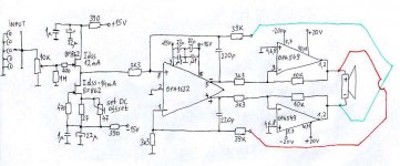
I took another shot at this idea (like in post #672) with inverting OPA549 and OPA1632:
SuSy amp sa inv. OPA549 - DIY Audio Forum
(it's our local, Serbian, forum but pics and schematics are self-explanatory).
With LM3886 you have to get rid of too much gain for my likings so I chose OPA549 and improvements in sound are noticeable. I listen to this amp two months already and I still enjoy it (I usually get bored by AB class amps after week or two).
Here is the final schematics:
Cheers!
Attachments
Last edited:
Juma,
I invite you to start a thread describing your SuSy amplifer. I for one would build a channel pair. It looks to be a simple yet very effective design.
Carl,
I cant' make myself to write the same thing twice
Here you have all the data you need so I suggest, if you are really keen to build this amp, to start a thread about it and I'll be here to give a helping hand
As far as description goes there is really nothing much to it - input buffer is a modified B1 (better drive capability - BF862 JFET has higher transconductanse and higher Idss, I also added a pot in Source of CCS JFET in order to set DC offset on the speakers).
OPA1632 is a great sounding, full differential amplifier that serves as a SE to bal. converter with gain and creates a SuSy feedback loops with OPA549s nested in.
OPA549 might not be the best power OpAmp per se, but in this topology (inverted, gain=3V/V, inside SuSy fb. loop) it gives better sonic results than LM3886.
I chose +/-20V for PSU because my speakers are 4 ohms - PSU voltage can be higher (up to +/-30V) if you have speakers with impedance that doesn't significantly drop below 8 ohms.
Cheers!
Last edited:
Hi Juma,
thank you for posting your schematic. I would like to try building it. I have four questions/points i was hoping you might help me with.
1. What would you think about replacing the discrete input buffer with an opamp? I was thinking of trying the LME49710HA. To compensate for the loss of the DC offset circuit I could select OPA549s with similar offsets. What do you think of this approach? I was favoring it because i have the part and it is a even simpler.
2. On the OPA549 + inputs you don't have any resistor to ground? Would this improve SNR?
3. You suggested that the OPA549 may not be the best choice, though it is better than the LM3886, do you have an alternative suggestion?
5. Do you use a DC blocking cap at the input?
thank-you
... I have four questions/points i was hoping you might help me with.
....
1. Yes, I used AD797 in previous version with success and amp's DC offset was about 5mV. LME49710 easily drives even 600 ohms loads (according to datasheet) but I don't know how does it sound. I suppose you'll find out
2. SNR is great already. OPA549 has JFET input. Resistor from +in to gnd might be used to equalize input bias currents ie. DC offset
3. No, I said it's not the best amp per se, but it's great choice in this SuSy GC project. If we want to step out of GC frame, I'd say we could use four good discrete amps instead of OPA549 - SumAsym 5.3 or even F5 - whatever one likes and has the means to build.
4. You missed that one
5. Yes I do. In my latest build, the amp is not integrated anymore, it doesn't have pot and input selector, just a buffer and 0.22uF WIMA MKP10 cap (input impedance of the buffer is 1M). I drive it with my BF862 preamp with no cap on it's output.
If we want to step out of GC frame, I'd say we could use four good discrete amps instead of OPA549 - SumAsym 5.3 or even F5 - whatever one likes and has the means to build.
Hi Juma, the above quote is the key point for me. Since I am a relative novice, I don't want to take on a more advanced project yet, but i still want good performance and a suitable challenge.
I have some follow-up beginner questions:
1. Why are the OPA549s used in inverting mode? I have read in chip amp data sheets that the inverted configuration can improve THD. Is this the case here as well? Do you have a simple explanation for why this is the true, the chip amp data sheets do not explain.
2. Why is the OPA1632 used at a relatively high gain and the OPA549 used at low gain(at least compared to a chip amp). Is this to take advantage of the nested feedback - it shifts the non-linearity cancellation to the higher performing device - the OPA1632. Is this why the OPA549 is better suited to this circuit than a chip amp (which has to be used at a higher gain)?
3. What do you estimate the power output of your circuit is? Have you considered paralleling OPA549s - i guess that could get pricey quickly.
Thanks again.
Last edited:
Volumes are written on that subject, but to make a long story short - OPA549 in inverting configuration gives more enjoyable sonic results (IME)...
1. Why are the OPA549s used in inverting mode? ...
OPA549 has wider bandwidth and accordingly, sounds better when used with lower gain and OPA1632 has to make up for that - nested loops can be tricky - many people wrote about that subject too (Walt Jung comes to my mind).2. Why is the OPA1632 used at a relatively high gain and the OPA549 used at low gain....
With PSU of +/-20V per side of a bridge we'll have about 90W (peak) at 8 ohms load and about 140W (peak) at 4 ohms speaker. Limiting factors are max. swing on the load (about 32V peak), max. current through the chip (8A continuously) and SOA of the chip (see the datasheet).3. What do you estimate the power output of your circuit is? Have you considered paralleling OPA549s - i guess that could get pricey quickly.
I use this amp to drive 4 ohms speakers (Canton CT-1000 and Epos M5) with no signs of overload (even into very loud levels) so I didn't feel the need for paralleling of chips.
bakpaosiomay,
what's your power supply voltage?
What's the Id through JFETs?
What else did you change (beside transistors in LTP)?
if you kept R16 at 14R it will give about 23mA through each JFET and it's far too much. Changing R16 to 68R will give 5-6mA through each JFET and that would be OK, and the Drain resistors would have to be changed to something like 2k2. As you see, the drop-in replacement is not a good idea if you don't know exactly what are you doing.
2sk246 is a low transconductance JFET and that makes it a poor choice for this differential pair (LTP) - you have 10k/620R voltage divider (attenuator) after it. 2sk170 or cascoded BF862 will give much better result here - if you are so keen on using a JFET
Last edited:
i used 20v supply i also changed the bias to 2.5 ma each jfetbakpaosiomay,
what's your power supply voltage?
What's the Id through JFETs?
What else did you change (beside transistors in LTP)?
if you kept R16 at 14R it will give about 23mA through each JFET and it's far too much. Changing R16 to 68R will give 5-6mA through each JFET and that would be OK, and the Drain resistors would have to be changed to something like 2k2. As you see, the drop-in replacement is not a good idea if you don't know exactly what are you doing.
2sk246 is a low transconductance JFET and that makes it a p
oor choice for this differential pair (LTP) - you have 10k/620R voltage divider (attenuator) after it. 2sk170 or cascoded BF862 will give much better result here - if you are so keen on using a JFET
so what do you think?
should i changed back to mpsa42 or something else maybe irf610?
i also think 20ma is to much for mpsa42
because my mpsa42 is very hot i cant touch it
is there a problem if i reduce the bias?
Last edited:
Hi Juma,
i've ordered the parts I didn't already have and i am designing a circuit board so the project is on the move.
When you ran the circuit with the AD797 at the input did you use with a gain of 1. Do you have any comments about the impact of having more/less gain with the input opamp than the opa1632.
Thanks
i used 20v supply i also changed the bias to 2.5 ma each jfet...
You obviously redesigned the circuit which metalman used. So it would be best to present your whole project - complete actual schematics, parts data (Idss of JFETs used), PSU details...
The more data you supply, more likely that you'll get appropriate help. It's going to be tough if we have to pull the words out of you
...When you ran the circuit with the AD797 at the input did you use with a gain of 1.
Yes, you can see that schematics in the post #672
Do you have any comments about the impact of having more/less gain with the input opamp than the opa1632.
First time I made this amp I chose AD797 to be the input buffer (voltage gain of 1) because it's great sounding chip able to drive low input impedance of the next stage (opa1632) and because I had AD797 ready. Now I happen to have a lot of BF862 and they make a great sounding input buffer too.
It worked great when amp was configured as an integrated amp - I didnt need additional gain (my DAC gives 1.7Vrms at its' output) - so I didn't use input opamp with more gain than 1. Of course, if you need more gain you can add preamp or change buffer to gain stage or change the gain of the SuSy feedback loop, feel free to experiment
Hi Juma,
have you measured the frequency response of your amp?
I am trying to model your circuit in Tina-TI to better understand the circuit. Presently, using the posted schematic, there is peaking between 10 and 20 Khz which is a result of the 220 pF cap.
I realize that models are always incorrect by some degree, but I am hoping you can give me some measurements so I can determine if the model is at all useful.
Tim
Hi okapi,Hi Juma,
have you measured the frequency response of your amp?...
no I didn't, I make that kind of measurements only if I have a problem with the circuit.
Of course, you can experiment with the value of that cap (it's there to prevent OPA1632 from oscillating) but I doubt that Tina will show you what's really happening there.
The only way to know for sure what's really going on, is to build it.
Last edited:
I want balanced inputs.
...
Can i just add another buffer or opamp on the negativ sida for the opa1632??
/JZ
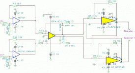
Hi zei,
of course you can. I used opa1632 as Single Ended to Balanced convertor (with one input grounded). You can use it as Fully-Differential amplifier (with signal on both inputs). Only thing to change is to lower the gain - instead of 39k resistors use 22k.
And yes, you'll have to buffer both inputs.
Hi zei,
here is the schematic with fully-differential (balanced) input.
I left out the PS coupling parts and pinout of chips, you have them in schematic in post #672.
Some part values are different in this new sch. - don't worry about that, the amp sounds better this way.
Cheers !
here is the schematic with fully-differential (balanced) input.
I left out the PS coupling parts and pinout of chips, you have them in schematic in post #672.
Some part values are different in this new sch. - don't worry about that, the amp sounds better this way.
Cheers !
Attachments
- Status
- This old topic is closed. If you want to reopen this topic, contact a moderator using the "Report Post" button.
- Home
- Amplifiers
- Pass Labs
- GC SuperSymmetry