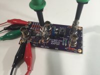
My OPA1622 adapter board is back from fab (OSH Park). The first day's soldering experiments with the VSON packages were unsuccessful; got pin-to-pin shorts in every case. Next attempts will be with a stencil and more tightly controlled temperature profile. The good news is, the test motherboard in post #152 works well. Both the analog and digital signal paths checked out fine using a scramble soldered emulator of the OPA1622 adapter board, plugged into the OPA1622's DIP10 socket.
Last edited:
If you are addressing the question to me (can't quite tell),How far are the PS caps and the feedback network resistors from the chip itself?
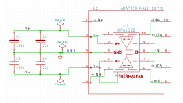
There are eight power supply capacitors, four per rail. Four of them are shown in post #76, as "C1, C2, C3, C4". The other four are shown in post #152 as "C2, C3, C4, C5" (the non electrolytics are on the back side of the board).
The feedback network is on the motherboard not the OPA1622 adapter board. We shall see whether this is disastrous in real life, or not. That's one reason for using BNC connectors: to search for VHF oscillation with scope and/or spectrum analyzer.
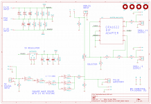
In post #152 the first half of the '1622 is configured as a unity gain noninverting buffer with no feedback resistors at all, and the second half is configured as a unity gain inverting amp using resistors R9 and R10. Both opamp halves include resistors in series with the output pin; those are R4 and R11.
There are good reasons for including all those components from Fig. 60 & 48 of the datasheet.
Also it has been mentioned elsewhere that SMD resistors of 0603 or smaller has higher distortion.
And ceramic caps are microphonic / piezoelectric.
All true, I used 1206 sized in a desktop headamp project for that very reason. Interesting comment about that from Hofer in one of his slide shows. This one is a bit of a trade-off for size. It plugs into a project that is only about 2.5x larger. The feedback caps will be COG of course and luckily those are available in 50V now in 0402 which will help with dV related things. The maximum swing will only be around 5Vrms. The other missing datasheet parts are on the board it plugs into.
Hey nice looking board of yours there.
")
Mark - interesting about the soldering!
This weekend I discovered that I've got a lot to learn about SMD soldering. I built nine of my OPA1622 daughterboards, which each have a grand total of five SMD parts (4 x 0805 caps + 1 x VSON-10 IC). The yield was eight dead boards and one working board. Ugh!
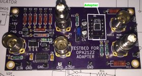
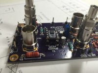
But one daughterboard does work; here are some photographs. I trimmed the through-hole leads that extend from daughterboard into the DIP-10 socket on the motherboard; they're about 300 mils long. Just enough to seat in the socket and stand off the board so the bottom-mounted bypass capacitors don't collide with the socket.
I used BNC sockets and BNC adapters, to connect my scope probes to the board with very little ground inductance (last photo).
Attachments
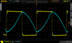
To debug the motherboard I build an OPA1622-thruhole emulator using an LM358 (!!) opamp. Here are the test results. If you ever wondered whether the LM358 is a crappy opamp, look no further.
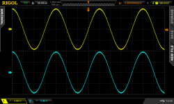
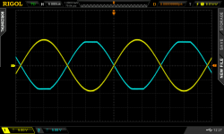
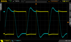
Why is crossover distortion so much bigger in the inverting amplifier than the noninverting? Because the inverting amplifier drives a resistive load (its 1K feedback resistor, R10) while the noninverting amplifier doesn't drive any load.
Why is crossover distortion so much bigger in the inverting amplifier than the noninverting? Because the inverting amplifier drives a resistive load (its 1K feedback resistor, R10) while the noninverting amplifier doesn't drive any load.
Attachments
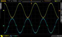
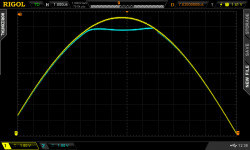
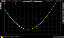
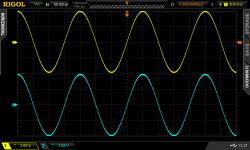
Here's the OPA1622 on my adapter daughterboard, amplifying 5 kHz and 30 kHz sine waves. Input = Yellow, Output = Blue. Supplies are plus-and-minus 10V for 5 kHz, plus-and-minus 9V for 30 kHz. My function generator doesn't pump out very large amplitude sinewaves, so I lowered the OPA1622's rails from 10V to 9V, to force it into clipping. Overload/clipping appears well behaved with no phase reversal on the output.
Attachments
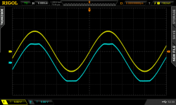
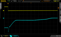
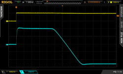
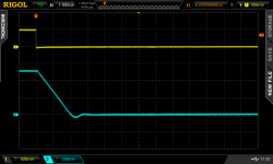
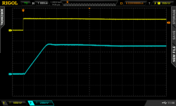
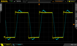
I ran a few square wave tests too. The motherboard generates 5V square waves using a 74AC "Advanced CMOS" logic chip, which gives quite zippy rise and fall times. These are attenuated 10:1 to drive the opamp inputs. Why? To keep the output small enough that it won't fry the input stage of a spectrum analyzer whose max rated input level is +20dBm. In case I ever try that.
The square wave testing was done with plus-and-minus 10 volt supplies.
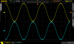
Square wave response of the OPA1622 was pretty good, but it can't keep up with a 3 MHz squarewave that switches between 0V and +0.5V. Go ahead and calculate a "small signal slew rate" from that photo, if you're in the mood.
Overall, it appears the adapter is working. I don't see any gross instability in either the inverting or the gain-of-one noninverting half (Rf = Rin = 1K).
The square wave testing was done with plus-and-minus 10 volt supplies.
Square wave response of the OPA1622 was pretty good, but it can't keep up with a 3 MHz squarewave that switches between 0V and +0.5V. Go ahead and calculate a "small signal slew rate" from that photo, if you're in the mood.
Overall, it appears the adapter is working. I don't see any gross instability in either the inverting or the gain-of-one noninverting half (Rf = Rin = 1K).
Attachments
There are good reasons for including all those components from Fig. 60 & 48 of the datasheet.
Also it has been mentioned elsewhere that SMD resistors of 0603 or smaller has higher distortion.
And ceramic caps are microphonic / piezoelectric.
Cheers,
Patrick
Certain ceramics are micro phonic but this will have no affect when used for decoupling, nor would the distortion...
That said use NP0/C0G in a small package and you don't have either problem, and these are ceramic.......
As they say in the R&D Fab, I've completed another cycle of learning in my SMD soldering process. This time the yield was 3 out of 3 (100% yield), which is an improvement over last time (1/9 = 11% yield). Better (stiffer) mechanical support of the flexible Kapton stencil during paste application, and better temperature-vs-time plus better monitoring, seem to have helped a lot.
I've taped out a rev.2 adapter PCB layout which ought to help even more, plus a rev.2 stencil layout with more attention given to the % coverage of the giant thermal pad underneath the chip. Both the new boards and the new stencil ought to arrive in about a week, and then I'll assemble some rev.2s and test them, to see whether they give the expected improvement.
I've taped out a rev.2 adapter PCB layout which ought to help even more, plus a rev.2 stencil layout with more attention given to the % coverage of the giant thermal pad underneath the chip. Both the new boards and the new stencil ought to arrive in about a week, and then I'll assemble some rev.2s and test them, to see whether they give the expected improvement.
OPA1622 as DAC I/V conversion
I am experimenting with a DAC buffer. I am using an ESS ES9018 with all 8 channels configured in parallell. This configuration demands the opamp to deliver up to 31mA of current to virtual ground trough the feedback resistor. To handle this current I have been using a LME49600 in the feedbackloop with a MUSES8920 opamp.
After reading this thread and the datasheet for the new OPA1622 it seems that this must be a better and simpler solution. Lower noise, lower THD and enough current capability.

Any comments on this implementation?
There will still be -1,65V DC offset on the outputs. This will be taken care of by an external circuit.
Any more luck with your soldering Mark?
I am considering making some converter boards similar to yours as well.
Armand
EDIT! Just saw your comment Mark. Congratulations on your success. Are you using a reflow oven? Also, what type of solder paste?
I am experimenting with a DAC buffer. I am using an ESS ES9018 with all 8 channels configured in parallell. This configuration demands the opamp to deliver up to 31mA of current to virtual ground trough the feedback resistor. To handle this current I have been using a LME49600 in the feedbackloop with a MUSES8920 opamp.
After reading this thread and the datasheet for the new OPA1622 it seems that this must be a better and simpler solution. Lower noise, lower THD and enough current capability.
Any comments on this implementation?
There will still be -1,65V DC offset on the outputs. This will be taken care of by an external circuit.
Any more luck with your soldering Mark?
I am considering making some converter boards similar to yours as well.
Armand
EDIT! Just saw your comment Mark. Congratulations on your success. Are you using a reflow oven? Also, what type of solder paste?
Last edited:
I used this hotplate from Amazon, along with this IR thermometer. The adapter PCB is a tiny little thing, 400 x 600 mils, which I place on an aluminum heat diffuser / easy to pick up carrier, a 3 inch length of aluminum bar stock from Home Depot. The aluminum bar goes on the hot plate, and the PCB goes on the aluminum bar. When soldering is complete, I use pliers to pick up the hot aluminum bar and place it on a plank of wood to cool.
So far I've only tried Kester 276 solder paste in tin+lead. Stencil is 3 mil Kapton from OSH Stencils.
I use my DMM as a tester. Continuity setting ("beeper") finds pin-to-pin shorts. Diode test setting, with DMM+ connected to OPA1622 pin 4, and DMM- connected to pin_under_test, finds pin opens. If the ESD protect diode isn't there, you've got an open pin. Just like the million dollar Teradyne testers do it at Texas Instruments and Analog Devices. If no opens and no shorts, I add the four 0805 capacitors to the bottom side, add the thru hole leads, and plug it into the motherboard for E_test. If it amplifies a 50 kHz sine wave, square wave, and triangle wave, thru both on-chip opamps, I declare it good.
The whole rig is nothing but basement-hobbyist, low tech gear.
Thanks for your tip Mark. I have been buying PCB's and steel stencils from gojgo.com. Stencils are $17 so it's not bad, but for hobby/test use OSH Stencils is a better option. I have an old reflow oven for my soldering needs.
Are you going to sell some of your PCB's in the near future?
Armand
Are you going to sell some of your PCB's in the near future?
Armand
I am experimenting with a DAC buffer. I am using an ESS ES9018 with all 8 channels configured in parallell. This configuration demands the opamp to deliver up to 31mA of current to virtual ground trough the feedback resistor. To handle this current I have been using a LME49600 in the feedbackloop with a MUSES8920 opamp.
After reading this thread and the datasheet for the new OPA1622 it seems that this must be a better and simpler solution. Lower noise, lower THD and enough current capability.
View attachment 546490
Any comments on this implementation?
There will still be -1,65V DC offset on the outputs. This will be taken care of by an external circuit.
Any more luck with your soldering Mark?
I am considering making some converter boards similar to yours as well.
Armand
EDIT! Just saw your comment Mark. Congratulations on your success. Are you using a reflow oven? Also, what type of solder paste?
I didn't think the ES9018 required 0V at the DAC outputs to perform its best, and in that case you could put a bias voltage on the non-inverting inputs of the OPA1622 to center the amplifier outputs at 0V.
Another breakout for the OPA1622
Thanks for the tip John. I will try to put a low noise regulator as the Vref. I have done some testing with one that gave me from 1,5-5nV/Hz in the 20Hz to 20kHz range. With that noise performance the effect on the amp should not be measurable. It also makes is very easy to supply both single ended and balanced output from just one little 3x3mm chip
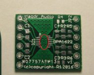
I am so eager to test this chip that I have made my own version of the breakout board as well. I must admit that I "cheated" a little and based my design a little on agdr's nice design in post #200. I hope thats OK agdr.
I used mostly 1206 sized SMD's and without a dedicated pin for the negative input resistor.
I also made the pads for the opamp fairly long. It makes it easier for hand soldering.
What to do while waiting for the boards?


Thanks for the tip John. I will try to put a low noise regulator as the Vref. I have done some testing with one that gave me from 1,5-5nV/Hz in the 20Hz to 20kHz range. With that noise performance the effect on the amp should not be measurable. It also makes is very easy to supply both single ended and balanced output from just one little 3x3mm chip
I am so eager to test this chip that I have made my own version of the breakout board as well. I must admit that I "cheated" a little and based my design a little on agdr's nice design in post #200. I hope thats OK agdr.
I used mostly 1206 sized SMD's and without a dedicated pin for the negative input resistor.
I also made the pads for the opamp fairly long. It makes it easier for hand soldering.
What to do while waiting for the boards?
Armand said:I hope thats OK agdr.
Definitely OK!
Anything I post on the forum I always hope other DIYers will use and improve on.Here is one mistake not to make, below. Be sure you have specified no solder mask under the chip! I missed that one.
On mine I didn't extend the bottom heat sink foil under the SMD parts out of concern for capacitive coupling between the parts via the plane, and/or capacitive coupling from the parts to that Vee plane. The heat sink plane on the bottom looks just like the dogbone on the top. But I'm probably just over-thinking it too! I know the cap coupling [10pF max?] is very small through the 1.6mm board.
I would be curious what johnc124 thinks about the issue. Is it best to have no plane under the SMD parts, a ground plane under them, the Vee/heatsink plane, or does it even matter?
I did find an answer to that question I had a few posts back about whether removing the solder mask over the rest of the heat sink foil improves thermal transfer. I found a TI white paper on thermal pads under chips and it states that the heat transfer is about the same with or without the mask on the rest of the foil. So probably best to leave it on to prevent corrosion over time.
Attachments
Last edited:
Hi John
I noticed quite significant performance drop for 1622 when supply goes down to +/-2.5V. Even on light loads (inverting configuration). I understand basic mechanics of this, but it is bloody sharp droop starting somewhere from ~+/-3.75V.
Would be curios to hear any insight on this.
Thank you in advance.
Last edited:
- Home
- Vendor's Bazaar
- New Audio Op Amp - OPA1622