And Sanyos are part of ONSEMI.
Try these.
Product Search Results
They do not has quite as low millercapacitance but all other parameters looks good.
Try these.
Product Search Results
They do not has quite as low millercapacitance but all other parameters looks good.
I think Fairchild makes substitutes for the Sanyos.
Yes. This what I am using on my amps for TIS devices
PNP = KSA1381
NPN = KSC3503
Yes. This what I am using on my amps for TIS devices
PNP = KSA1381
NPN = KSC3503
those I can get easy from Mouser
") and even though they come from outside EU, I know they are in my mailbox within a few days
and even though they come from outside EU, I know they are in my mailbox within a few daysHi LC,
Very nice ,simple,easy to build design.I like it
The closed loop gain depend up on different feedback path for upper and lower half cycles.So these feed back resistors are very close in values.Better to use matched one or use 0.1% tolerence .Even 1% variation make 4% gain difference (in worst case)and become assymetrical in each half cycles.
Best regards
joshvi
those I can get easy from Mouser
The ones from mouser are two different gain ranges.
I also have them, but mine are in the same range.
.... two different gain ranges.
ahh, you mean the SA(PNP) is hfe1-E grade, and SC(NPN) is D-grade
couldn't find it before bit I see it now, hfe D-grade 60-120 dc gain, E-grade 100-200
thanks!
The closed loop gain depend up on different feedback path for upper and lower half cycles.So these feed back resistors are very close in values.Better to use matched one or use 0.1% tolerence .Even 1% variation make 4% gain difference (in worst case)and become assymetrical in each half cycles.
You nailed it....
That s the main problem with separate FB return since 1% mismatch
in the two FB resistors can increase distorsion by 10dB.
You nailed it....
That s the main problem with separate FB return since 1% mismatch
in the two FB resistors can increase distorsion by 10dB.
That's why I measured all feedback resistors (also all other parts crucial for OLG, CLG) in my SSA, CSA, VSSA, to 4th decimal matching with my Fluke ... one of the reasons I bought Fluke in the first place.

Last edited:
Where 50uV and 2V derive from?
supply ripple in AC signal ground (10uF||2,2mF) ratio to feedback voltage
That's why I measured all feedback resistors (also all other parts crucial for OLG, CLG) in my SSA, CSA, VSSA, to 4th decimal matching with my Fluke ... one of the reasons I bought Fluke in the first place.
Other parts than theses ones are not that critical as they will be compensated
by GNFB , the only other details is to have quasi matched currents running
through the two input transistors but this is also less critical than the said
resistors precision that should be matched in the 0.1% range , quite possible
even without a Fluke....


Hi Lazy Cat, thanks for sharing...
this is basic question, I hope you don't mind
It is very difficult to find matched high hfe input pairs, output pairs, or driver (if needed)?
Can I use matched pair(2SA/SC) but low hfe not more than 400, what is the problem that I will see then?
this is basic question, I hope you don't mind
It is very difficult to find matched high hfe input pairs, output pairs, or driver (if needed)?
Can I use matched pair(2SA/SC) but low hfe not more than 400, what is the problem that I will see then?
Hi John 
Yes, if you didn't started with any previous SSA-s, it is convenient occasion now to start this simple topology with VSSA, probably the least demanding.
Well my BC input pair transistors have hFE=620, not so much higher than yours. Current gain is important mainly when load is connected. Load current has influence to all previous stages, since it loads them with current all the way back to the input signal. Load current influence is complex, meaning impedances of all stages reveals their character, mostly capacitive, causing phase shifts between signal voltages and currents. Since we have only three stages amplifier, gain of each device is very important to get serious output current capability, without getting into saturation of one stage, while other two would still have some reserve if properly driven. I suggest you to start with the input pair you have and if the load connected will cause too much stress (current based distortions), my advice would be to try to find higher hFE transistors.
Regards Andrej
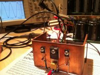
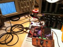
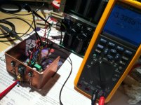
VSSA prototype is working, very well I could say. All DC and AC conditions stable, turn on without any swing, imediately zero DC on the output. Bias setting very linear, no jumps whatsoever. Without any compensation 10 Vpp 25 MHz oscillation, two 12 pF caps on VAS makes it completely stable.
Pics showing 38,4 Vpp, 1 Mhz sinus signal, tested at max 3 Mhz, still no sign of smallest attenuation.
The only problem I noticed is thermal bias PTC because of VSA BJT's located on the same heatsink as the outputs. Solution is to use reference adjustable zener for bias spreader or relocation of 2SA/SC to separate heatsinks. My wish is of course to have them on the main heatsink because of PCB-module compactness. Any suggestions?
Attachments
Last edited:
.....
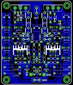
Hi Alex, nice to see you continue to draw layout. According LC schematic the left one 1uF near 2sk1058 should be after fuse and at right side the 4x220µ should be befor the fuse. Yet i don't know if this make a difference but shoundn't be the 1uf the more we can near Fet drain?
Marc
VSSA prototype is working, very well I could say. All DC and AC conditions stable, turn on without any swing, imediately zero DC on the output. Bias setting very linear, no jumps whatsoever. Without any compensation 10 Vpp 25 MHz oscillation, two 12 pF caps on VAS makes it completely stable.
Pics showing 38,4 Vpp, 1 Mhz sinus signal, tested at max 3 Mhz, still no sign of smallest attenuation.
The only problem I noticed is thermal bias PTC because of VSA BJT's located on the same heatsink as the outputs. Solution is to use reference adjustable zener for bias spreader or relocation of 2SA/SC to separate heatsinks. My wish is of course to have them on the main heatsink because of PCB-module compactness. Any suggestions?
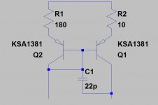
Q2 on heatsink. Q1 on top. But the gain is reduced 2.6 times
Attachments
- Home
- Vendor's Bazaar
- VSSA Lateral MosFet Amplifier