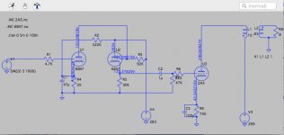
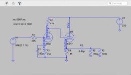
I've started receiving the parts to make a 6SN7 line stage inspired by the Wright WLA12 (VA/CF). This will not be a clone, but rather a somewhat open-ended project beginning with the Vacuum Tube Valley (VTV) Octal Line Stage published in VTV Magazine issue #11 (Spring 1999) (schematic attached). The plan is to build the line stage as originally published, listen, and adjust to my system and taste by improving the known-to-be-problematic power supply (it puts out 330V B+ rather than the 370V as published, etc.), tweaking component values and operating points, and eventually adding a 6EM7 high voltage series pass regulator.
I chose the VTV because it's of the same topology and same era as the Wright model and the Bottlehead Foreplay. Confession: this is also a kind of search for Lost Time, back to my first introduction to tube hi-fi in 2001-02, when I heard the Wrights, so the design and sounds "of the period" are part of the curiosity here.
This will also be my first point-to-point and from-schematic build, having previously made two half-kits (Tubelab SE 300B and VTA PH16). My hope is that this thread will be useful to other newbies who want to take on a project like this.
First question: What is the purpose of the 1M resistor between the output coupling capacitor and the output RCA jack? I've simulated the signal section in LTSpice, and the sine wave in the transient analysis looks beautiful without the 1M resistor yet is horribly distorted with it. Is it necessary to use it?
Attachments
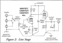
What is the purpose of the 1M resistor between the output coupling capacitor and the output RCA jack?
I've simulated the signal section in LTSpice, and the sine wave in the transient analysis looks beautiful
without the 1M resistor yet is horribly distorted with it. Is it necessary to use it?
Mainly, it provides a path to ground for the output coupling capacitor.
It won't be a source of distortion, so the simulation must be at fault.
Are you sure that the value of the resistor is 1M, and not, say, 1k.
There's another resistor in the amplifier's input, for similar reasons.
Last edited:
Are you sure that the value of the resistor is 1M, and not, say, 1k.
Hi rayma,
The schematic I attached reads "1 Meg" at that position, so I assumed it was 1M. I've seen other preamp designs that feature this, even some up to 1M5.
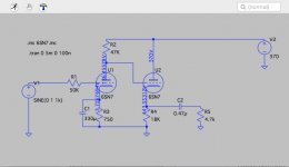
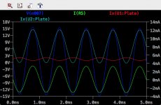
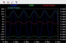
OK, so trying to figure out what wattage rating I'd need for the 1M resistor, the blue line in the transient graph (attached) shows a voltage swing from +15V to -15V on the meter placed just before the 4.7K load resistor (I set up this model as if it were powering a Wright WPA 3.5, which has a 4.7K input resistor).
To calculate the dissipation of a 1M resistor at that voltage, 15^2 / 1,000,000 = .000225W. Or, if we take the full swing, 30^2 / 1,000,000 = .0009W.
So would a 1/4W resistor be OK?
Attachments
would a 1/4W resistor be OK?
Sure.
This image shows 4.7k for the output load resistor, which could cause distortion,
as well as reduced LF bandwidth.
It appears that the 4.7k is actually the amplifier's grid stopper resistor, not the one to ground [grid leak].
https://robrobinette.com/images/Guitar/HowAmpsWork/Triode_Tube_Circuit_with_Signal_Path.jpg
I think the amplifier's input resistor to ground is at least 100k, or larger. Try it with that value.
Last edited:
I updated the LTSpice schematic (attached) to reflect the 330V B+, the 1M resistor after the output capacitor, and a 100K load representing the input resistance of the WPA 3.5 as seen by the preamp.
The graph now shows quite bad distortion.
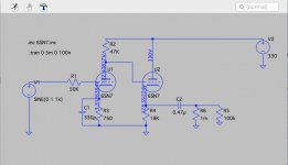
How did you get the 100K load resistor value? The 4.7K in the WPA 3.5 (LTSpice schematic also attached) is indeed the grid stopper of the input 6SN7.
Looking at the 6SN7 datasheet, I don't find a grid resistance value, though there is a grid circuit value of 1-2.2M, which doesn't seem right here.
The graph now shows quite bad distortion.
How did you get the 100K load resistor value? The 4.7K in the WPA 3.5 (LTSpice schematic also attached) is indeed the grid stopper of the input 6SN7.
Looking at the 6SN7 datasheet, I don't find a grid resistance value, though there is a grid circuit value of 1-2.2M, which doesn't seem right here.
Attachments
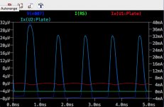
The graph now shows quite bad distortion.
This circuit is somewhere in the ballpark, and shouldn't distort badly.
> 1M resistor after the output capacitor
Is that "meg" or "milli"?
In *my* SPICE, upper/lower-case does not matter (FORTRAN guts), so if you want Meg you have to say "Meg". Else you get milli.
Which sure would crap-up a signal expecting many-K loading.
Power dissipation? You are unlikely to run much 1V signal into a power amp. 1V^2/1Meg. This is literally a microWatt. Even with extreme overdrive, hardly a milli-Watt. You pick a resistor big enough for your fingers, or whatever size is lowest-price, or prettiest colors, not by power.
The 1Meg bleeds-off charge on the output cap. Otherwise if left unconnected, cap leakage will bring the output up over 100V DC. If you plug-in at this point, the power amp POPs as it discharges the output cap. This may not be "essential" in hi-fi, where you rarely change connections and never while power is on (tho without the bleeder, the DC may persist a long time). It becomes somewhat essential in music amps and studio work, where plugs are moved often.
Yes, there is 1 milli-ohm load now, not 1 Meg.
Concerning the schematic in general, you could remove C1. Then you get lower gain that is maybe more suitable for a line level pre amp, but also better linearity (lowe THD).
This difference in supply voltage is practically meaningless.
Concerning the schematic in general, you could remove C1. Then you get lower gain that is maybe more suitable for a line level pre amp, but also better linearity (lowe THD).
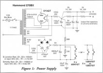
(it puts out 330V B+ rather than the 370V as published, etc.)
This difference in supply voltage is practically meaningless.
Last edited:
While the difference in B+ rail voltage is (as has been pointed out) probably NBD, a simple way to raise the rail voltage is by using a 5AR4 [low forward drop], instead of a 5Y3 [large forward drop]. Further tweaks are: eliminate the 100 Ω resistor between the rectifier and 1st filter cap., reduce the 1st filter cap. to 47 μF., and increase the paired 100 μF. parts to 150 μF. each. I doubt you will get to 370 V., but you will be close. 270 VRMS is 381.8 V. peak, which leaves little "slack" to take up the inevitable losses.
I'm planning the layout and have a couple questions about signal grounding.
1. It would be mechanically convenient to place a small tag strip between the two 6SN7s and solder all of the cathode resistors and capacitors, from pins 3 and 6 of both channels, to a single lug, and then run a single wire to the star ground point.
2. It would also be convenient to solder all the RCA ground tabs together (from both channels, the 4 input pairs as well as the output pair) to a single bare wire that runs to the star ground point.
I think this is desireable for reducing the number of wire runs to ground and lessening the chance of ground loop hum, but not sure if it could result in crosstalk or other undesirable behaviors.
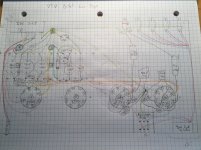
Attached is a scale drawing of what I plan to do, as seen from the bottom as if I were working on it, plus the schematic again for reference. Chassis is a 6 x 10 x 2 Hammond aluminum.
Star ground point is top left, near the IEC inlet. Pea green pencil shows wires that go to ground (the darker green is the 6.3V secondary that goes from PT to the heater supply).
The PS is done on 4 parallel, 6-lug tag strips. I could only find radial leaded caps in the values I needed, so it's as if you're looking at them from the top down.
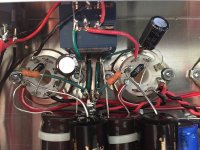
The 6EM7 socket is currently empty because I'll try it as an HV regulator in the future.
Signal goes from four pairs of RCA inputs to a 4 pos 2 pol selector switch before heading to the Alps 100K stereo volume pot.
My main concern is the single lug between the 6SN7s that connects the cluster of B+ & cathode caps and resistors from both channels, plus the vol pot signal ground. A thick ground wire will then connect the cluster to the star ground point.
Does that seem OK?
This is my first point-to-point build, and I really appreciate your feedback.
Thanks!
Star ground point is top left, near the IEC inlet. Pea green pencil shows wires that go to ground (the darker green is the 6.3V secondary that goes from PT to the heater supply).
The PS is done on 4 parallel, 6-lug tag strips. I could only find radial leaded caps in the values I needed, so it's as if you're looking at them from the top down.
The 6EM7 socket is currently empty because I'll try it as an HV regulator in the future.
Signal goes from four pairs of RCA inputs to a 4 pos 2 pol selector switch before heading to the Alps 100K stereo volume pot.
My main concern is the single lug between the 6SN7s that connects the cluster of B+ & cathode caps and resistors from both channels, plus the vol pot signal ground. A thick ground wire will then connect the cluster to the star ground point.
Does that seem OK?
This is my first point-to-point build, and I really appreciate your feedback.
Thanks!
Attachments


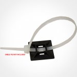
I thought I'd use double sided mounting tape to secure them to the chassis. Seem OK or bad idea?
Not as elegant as the adhesive cable mounting pads, but it would work in a pinch.
jeff
Attachments
Not as elegant as the adhesive cable mounting pads, but it would work in a pinch.
jeff
Didn't know about those. Thanks!
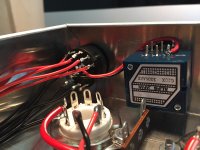
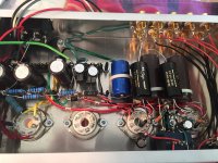
The build is nearly complete. All that's left to do is wire the IEC inlet and finish grounding the PS, and then test it.
I did a lot of reading about grounding schemes, and ended up using a combination bus bar and star format.
All the RCA returns (input and output) are on the same bus bar, an 18AWG solid copper wire that I stripped and tinned. I was concerned about grounding the inputs and outputs on the same bus, but Roy Mottram does that on his preamp builds, so I figured I'd try it and then separate them if there's a problem.
For the 6SN7s, I kept the two channel grounds separate and followed the schematic (see post #13 above) rigorously. There is a 2-tab terminal strip next to each 6SN7, with an 18AWG solid wire connecting the two tabs. The 750R cathode resistor and anode bypass cap attach at one tab while the 18K cathode resistor is at the other. Instead of soldering each volume pot ground to the lug with the 750R cathode resistor in each channel, I soldered them to one wire which in turn goes to that lug in the left (righthand in the pic) channel). The two 18AWG wires on the tag strips are then soldered to a central 12AWG solid THHN wire that goes to the star ground point at one of the PT mounting bolts.
I considered tying all the cathode resistors and caps to one bus bar or even to one lug, but figured they might behave better if their currents were separated upstream before joining the big river to ground. I was worried about ground loop hum forming there because of the two closely parallel tracks (even though they're only an inch long), so we'll see what happens.
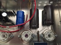
In the PS, I ended up mounting the caps vertically, bending the leads so they'd sit low enough in the chassis, and also covering the leads with shrink wrap to isolate them from bolts and the chassis.
And thanks again to Jeff for the tip on the adhesive zip tie mounts. They were only a couple bucks at Home Depot and provide a secure mounting connection plus the added bonus of space for fitting wires under the huge anode bypass caps.
Life would have been easier if I'd done this in a larger chassis, but it'll fit the aesthetic of the other components I've made, being the same size (6 x 10 x 2) as the pair of phono preamp chassis.
I did a lot of reading about grounding schemes, and ended up using a combination bus bar and star format.
All the RCA returns (input and output) are on the same bus bar, an 18AWG solid copper wire that I stripped and tinned. I was concerned about grounding the inputs and outputs on the same bus, but Roy Mottram does that on his preamp builds, so I figured I'd try it and then separate them if there's a problem.
For the 6SN7s, I kept the two channel grounds separate and followed the schematic (see post #13 above) rigorously. There is a 2-tab terminal strip next to each 6SN7, with an 18AWG solid wire connecting the two tabs. The 750R cathode resistor and anode bypass cap attach at one tab while the 18K cathode resistor is at the other. Instead of soldering each volume pot ground to the lug with the 750R cathode resistor in each channel, I soldered them to one wire which in turn goes to that lug in the left (righthand in the pic) channel). The two 18AWG wires on the tag strips are then soldered to a central 12AWG solid THHN wire that goes to the star ground point at one of the PT mounting bolts.
I considered tying all the cathode resistors and caps to one bus bar or even to one lug, but figured they might behave better if their currents were separated upstream before joining the big river to ground. I was worried about ground loop hum forming there because of the two closely parallel tracks (even though they're only an inch long), so we'll see what happens.
In the PS, I ended up mounting the caps vertically, bending the leads so they'd sit low enough in the chassis, and also covering the leads with shrink wrap to isolate them from bolts and the chassis.
And thanks again to Jeff for the tip on the adhesive zip tie mounts. They were only a couple bucks at Home Depot and provide a secure mounting connection plus the added bonus of space for fitting wires under the huge anode bypass caps.
Life would have been easier if I'd done this in a larger chassis, but it'll fit the aesthetic of the other components I've made, being the same size (6 x 10 x 2) as the pair of phono preamp chassis.
Attachments
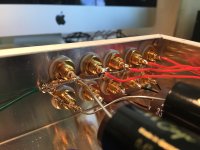
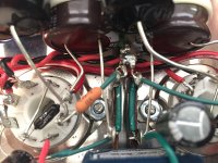
I hate to be the one to say this, but the quality of your soldering doesn't look adequate. Are you able to see this stuff clearly? If not, consider picking up a head-mounted magnifier of some sort. It would be a shame to expend so much effort and end up with poor results because of bad solder joints.
Build is finished and point-to-point connections all check out. I also went over all the cold-looking joints with a larger tip and more heat, getting better welds.
I powered it on with no tubes, in order to check the heater supply voltage of the 6SN7s, which should be 6.3V. My digital multimeter reads 19.6VDC and 43.5VAC across the heater terminals of each tube.
I tried to measure the voltage coming out of the 6.3V tap of the PT by placing the probes where the green wires connect the beginning of the heater supply. It reads 7.1VAC.
Are these voltages likely to be off with no tubes in place?
Re: the excessively high 43.5VAC at the heater terminals: I wonder if I used used the wrong diodes? The VTV article states "Si Junction Rect (1N5401 or equiv 50V, 3A)." I used this 1N5401 rated at 100V, 3A at Mouser:
http://www.mouser.com/Search/ProductDetail.aspx?R=1N5401-TPvirtualkey54720000virtualkey833-1N5401-TP
- Status
- This old topic is closed. If you want to reopen this topic, contact a moderator using the "Report Post" button.
- Home
- Amplifiers
- Tubes / Valves
- VTV Octal (6SN7) Line Stage Build --> Mod