DIY way to check working voltage of audio power transistors
Is there a simple way by which we can select higher working voltage power transistors from a lot .
If we make a variable unregulated supply by using a variac in the primary of the power supply transformer , check the transistor using a current limiting resistor in series and measure the breakdown voltage using a digital voltmeter.
will this work ?
can anyone give some more simple ideas
If you have a 100V power supply or supplies you could wire in series it would be easier. I would use a relatively high value resistor say 47k as there is the possibility of damaging the device.
In the old days the maker would do the selection i.e a TIP31A was a 60V device a TIP31B was an 80V device and a TIP31C was a 100V device.
I suspect you are wanting to push the device beyond the data sheet limits. There is usually some margin😀 but reliability may be compromised
In the old days the maker would do the selection i.e a TIP31A was a 60V device a TIP31B was an 80V device and a TIP31C was a 100V device.
I suspect you are wanting to push the device beyond the data sheet limits. There is usually some margin😀 but reliability may be compromised
Gosh, I forgot to say you need the correct polarity DC supply. Your proposal would apply unisolated AC which is not a good idea and is possibly dangerous.
HIGH Vcex
Hi Rajeev, you must read about fundamental electronics and semiconductors The Vce max depends on temperature,shematics(Rbe) and many others so you can not rely on one measuring with some shematics-dont push your luck!
Hi Rajeev, you must read about fundamental electronics and semiconductors The Vce max depends on temperature,shematics(Rbe) and many others so you can not rely on one measuring with some shematics-dont push your luck!
You are right Rope,
I knew that the devices may get destructed on breakdown testing, but I still wanted to try and see if there is a method,
Consort says that in old days they used to select Tip series in this way, Is that really possible ??
In another thread DJK had said that his friend had made the leach amp with selected transistors of higher working voltage 20 years ago which is still working ,
My problem is that here in India it is very difficult to get devices , specially for DIY purposes ,some replacement devices are avilible for professional amps but there rates are sky high , hence we have to use various alternative nos for our application , hence I got tempted to find out if there is a simple way to select devices and I want select devices which can withstand only 20 % more than the specified voltages
not worth it
i damaged several power trannies this way, i used very high series resistors, 1meg, yet i still damaged them...so i never tried again...they were unmarked to3 power trannies, i was able to get the breakdown voltage alright, but then after that it had leaks...
i damaged several power trannies this way, i used very high series resistors, 1meg, yet i still damaged them...so i never tried again...they were unmarked to3 power trannies, i was able to get the breakdown voltage alright, but then after that it had leaks...
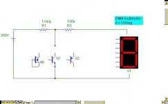
To test breakdown, use setup below. i tested many tranistors this way, no damage...important: no capacity at collector, this would make a avalanche peak current and destoy the dut. when testing mosfet, connect always (!!) gate to source before test.
to see temperature effects, watch voltage while heating up the dut with a solder iron.
with base open, voltage is VCEo.
to see temperature effects, watch voltage while heating up the dut with a solder iron.
with base open, voltage is VCEo.
Attachments
Don't use dc supplies directly.
To ensure that you do not bust the transistor , charge up a very low value capacitor ( maybe 0.1uF) and apply that through a switch to the device under test. Obviously the charging source for the capacitor must be disconnected while testing. A DPDT switch can be wired to achieve this. One contact opens while the other closes.
That way when the transistor breaks down at VCEO , there isn't much charge left to blow it. I've done this without blowing transistors . The DMM must be set to 'HOLD'and of course the series resistor must be there.
Use a low value resistor ( 1K?) between the dc supply and the 0.1uF cap to avoid a spark.
It was long ago and I can't remember what cap value I used. It was low however.
Cheers.
rajeev luthra said:You are right Rope,
I knew that the devices may get destructed on breakdown testing, but I still wanted to try and see if there is a method,
The old type 575 and 576 curve tracers use a variac powering a rectifier. no capacitor..
There is a selectable series resistor, the selector knob has on it maximum dissipation that the combination of voltage and resistance can deliver to the device under test.
Keep the dissipation to less than half a watt to a 1/10 th of a watt, and you most likely will not destroy the power device. Keep the current under 10 uA, and you will be safe, 100uA for power devices.
Bipolar, always tie base to emitter, mosfet, gate to source.
For bipolar devices, there is an additional issue...
The base width of the device is always a function of the device speed, and sat gain specs. The higher gain, faster devices will have thinner base diffusions..
You can certainly operate a device beyond it's designed values, as long as you remain below the breakdown levels...but you will not be able to easily test the device's ability to resist punch through, a rarely discussed failure mechanism, as most designers don't exceed design numbers..nevermind secondary breakdown, which gets nasty in the higher voltage regime.
Punch through causes a very high gain area under one of the emitter fingers, and causes thermal runaway in that spot, this runaway will not be at large currents, typically I've seen this kill a 250 mil square device with 10 milliamps current. For normal devices like 2n2907, I've seen it happen as a result of a defect in the primary mask from wafer fab, causing every fourth device on the wafer to fail. For power devices, it can happen directly under one of the bonding wires, as there is a concentration of stress under that that can push the depletion zone down. For RF and switching devices, it's nature of the beast, as the base width is minimized for speed.
Detection of punch through can be done by comparison of the BVCES vs BVCBO...the breakdown between the collector and base will have one value...if the breakdown collector-base with the emitter tied to the base is a lower voltage, the device is punching through...do this test at 10uA, and it will be non destructive.
Most manufacturers do not know where their devices will do this, or even if they do it at all..and they will destroy the devices during datalogging if they perform the normal BVceo test..so they typically do not do that, but simply a pass/fail at the maximum voltage of the device.
Keep below 10 uA, and you'll not destroy any..
Cheers, John
PS...well, you asked...

joan2 said:i damaged several power trannies this way, i used very high series resistors, 1meg, yet i still damaged them...so i never tried again...they were unmarked to3 power trannies, i was able to get the breakdown voltage alright, but then after that it had leaks...
A PN junction can only withstand a certain voltage, depending on how it is made. Exceeding this voltage even with a uA of current, the voltage will arc accross the junction and shoot a hole right through the barrier. After this, the reversed biased PN junction will have a leak through this hole. It can be a very small leak, but the charactoristics of the device will go right out the window, and then it will find its way to the trash can. 😀
Some datasheets of diodes include reverse biasing current versus voltage figures for various temperatures and these figures show that PN junctions go progressively leaky as the voltage and temperature increase. For some devices leakage current may be as high as 1mA at the rated breakdown voltage
1uA to 10uA currents are not likely to be dangerous for power devices since most of them reach these leakage currents well below its rated Vce at 25ºC. Some devices are rated at leakage currents as high as 500uA@200V@25ºC [look for example at MJ15025 datasheet]
I have no experience with C-B breakdown but I've experienced B-E breakdown in switching circuits [at turn off] and also for measurement purposes [to determine how much reverse biasing is safe during turn-off] and it was never destructive at low currents. I've used currents as high as 10mA for that purpose and apparently those junctions worked like a low power zener [usually 7 to 15V], no beta or Vbe changes were appreciated after testing
cunningham said:
A PN junction can only withstand a certain voltage, depending on how it is made. Exceeding this voltage even with a uA of current, the voltage will arc accross the junction and shoot a hole right through the barrier. After this, the reversed biased PN junction will have a leak through this hole. It can be a very small leak, but the charactoristics of the device will go right out the window, and then it will find its way to the trash can. 😀
That is an entirely incorrect statement...
In point of fact, there is a very good possibility that every single solitary pn junction device that is used on this planet has been subjected to a reverse breakdown test in the course of manufacturing and quality testing..
All standard construction pn diodes, after the lead/moly (or tungsten) brazed unit has been metallurgically bonded to the die, leads have been put on and the passivation covering the edge of the die (the sandblasted bevel), are subjected to reverse current in the test and binning process...does everyone think that they design 50, 100, 200, etc. devices, and produce a run of them??? NOPE...
They produce mass quantities of devices, with the highest voltage targeted...then they toss the entire batch into a vibratory hopper, and automatically test vf, ir, and bvr...once tested, the units are binned according to the specifications they pass..For a typical FER line at 200 volts, the prime units are sold as 200 volters, then all that fail that bvr are assigned to the 150, 10, or 50 volt bins, based on test...but all are bvr'd....
Planar devices are a tad different in passivation scheme..they can be tested to bvr on the wafer, as the breakdown zone has been forced away from the edge of the device by a deeper diffuson along the periphery. Regular silicon diodes have the edge bevelled to decrease the surface gradient in an effort to force the bulk of the device to breakdown before the edge...if the passivation is not good, contamination from the environment can get in, causing the device to breakdown in a very small point..that is a bad device..
Planar devices, mosfets, npn's, pnp's, zeners, signal devices, every single one of them are binned based on test results...very good manufacturers with excellent process control at the diffusion level will not have to bvr the entire wafer, but simply apply rated reverse to assure the device doesn't draw current in excess of the spec. If the device line is very difficult to make, they will have to do so to bin the product..
What you describe is totally incorrect for standard pn junctions...HOWEVER, it is absolutely, and totally, dead on accurate for the isolated gate structures of a mosfet, for silicon capacitors, and for some fiber optic termini I tested back in '84 (at 600 dollars apiece, I certainly wasn't gonna test the designer's assumption..). Reverse breakdown there will destroy the device.
If a pn device fails as a result of 1 or even 10 to 100 uA reverse bvr current, the device was bad and deserves it's fate...survival of the fittest..
Cheers, John
PS....ummmm, btw...does anyone really believe that the blister pak devices that are available at retail....are the prime units that have passed all quality specifications????
Back in '81, my employer would take the devices that failed incoming test specifications at THREE consecutive customers, put them into a large box, and sell them to certain companies by the POUND...(they made 4 million diodes a day back then...that box was big, even with ppm level quality..) The low tier customers would derate the device, either voltage or current, and package them....without any test capability whatsoever!!!
Reject categories included bvr, vf, ir, marking permanency, and...GET THIS!!!!!! cathode band on the wrong side of the device....DUH, no wonder the cap blew up.....test the semi's first...or caveat "empty"....

I would like to thank Stephen Mantz,consort_ee_um , alfsch , ashok , jneutron , rope , joan2 , Eva, & UrSv for the help,
The method shown by alfsch works and is most simple, at first my DMM did not read DC voltage as I had used only one one rect diode but later , I made a bridge and all was ok , I have tested only one one device and it did not get damaged , it is late at night now , my wife has already called me once , hence I will do the rest of testing later .
ps- ashok where are you , in India or the US
Hi
Today I added two crocodile clips with wires , to the breakdown tester as per alfsch s circuit, now it is easear and faster to connect the device under test . I also tried the 0.1 mfd condenser as mentioned by Ashok but I am too slow in my testing , as the cap discharges too soon , either I need a better quality cap or the value should be higher , anyway now that does not matter as the circuit works fine without the cap and there is no device failure , I hope it is not too premature to say this as I have not tested the devices actually in an amp as yet ?.
I have learened a lot by the text by jneutron & Eva .
I am quite surpurised to see the breakdown voltage variation in devices of the same number , I have tested NPN & PNP both and not one device failed , I also noticed that with a 100 ohm resistor between emitter & base the breakdown voltage increased by 20% in many transistors , but in some it increased by only 2%, all the devices were same no & make , I do not understand why this differance ?.
My power amp has 100ohms resistor between emitter and base of the output transistors , I would like to know if I have tested a breakdown of 100v of a device , which is 120v with the 100E resistor, what is the maximum supply voltage I can go to with these devices if it is a class AB amp with a + - supply
Hi Rajeev,
You should consider the maximum possible supply voltage that you might get. While the normal supply is 230 volts in your area , you should consider that it is not stable and can go up quite a bit. I would take 265 volts as a max value and see what dc supply voltage that would result in. Use that as your transient max voltage that would appear across the transistor.
I think the following might have been mentioned earlier.
The max voltage seen by the transistor is twice your +/- supply voltage. So +/-60 volts supply will be 120 volts across the transistor. Then again on no load you could get that. But on load that will not happen as the supply voltage will fall due to transformer losses. Under idle conditions it will however be just 60 volts or with some music it will be that many volts added to 60. At average listening levels you might have just 70 to 80 volt peaks .
If I were you I would use a 10% margin above what I said above. Having to replace devices in the field or on the service bench should be avoided . It's a waste of time and money for everyone. You probably want higher Vceo just to get more power out of the amp . A better solution is to use a bridged output amp. You will need lower supply voltages ( much safer ) and only have to handle higher current which can easily be done with parallel devices. You could get probably over 200 watts rms into 8 ohms with a +/-42 volt supply.
When transistors are fabricated in large numbers on a large wafer , they are all not exactly the same due to production variables. Physically they might be the same but performance will vary. With a very tightly controlled process they may get a batch with close tolerances. But in a facility ( China?) where they might not be so careful , the match between devices can be quite poor.
We do get a whole lot of 'stamped' brands out here. That could be the reason for your readings varying wildly. Besides this they might not be segregating the tested devices by performance. It makes it cheaper but unpredictable at the limits of their ratings.
Most equivalents from the East are probably just generic and not the same device. They do however come with known type numbers.
I am in India ... ( at the moment ).
Cheers,
Ashok.
rajeev luthra said:I am quite surpurised to see the breakdown voltage variation in devices of the same number , I have tested NPN & PNP both and not one device failed , I also noticed that with a 100 ohm resistor between emitter & base the breakdown voltage increased by 20% in many transistors , but in some it increased by only 2%, all the devices were same no & make , I do not understand why this differance ?.
My power amp has 100ohms resistor between emitter and base of the output transistors
There will always be bvr variation in the devices..sometimes, there is a large variation on a single wafer of product.
Even if the units have the same date code stamp, the devices can be from many different wafers, different areas of a single wafer, and even different diffusion runs..all will affect bvr. From one wafer, I have seen a ten volt variation for 40 volt devices, although they were running about 80 volts..
RE: the 100 ohm resistor:
When you test BVceo, you also have to include the leakage that travels from the collector to the base,, as that leakage is injected into the base, and amplified by the gain of the device. When you put a resistor from the base to the emitter, you bypass the active junctions with that leakage. I think the resistor will be a better test for you.
(btw..nomenclature for testing is: BVceo
BV=breakdown voltage
from "c"
to "e"
the third terminal (base, in this case) is "o" or open.
So your test is not BVceo, but BVcer
Cheers, John
@rajeev, look at my circuit, it has 300V DC as source. i use for simple testing the mains phase in series with 22k (for safety) and a 1n4007, then a 0.22uf /400V foil cap to ground. this gives the 300VDC. you can test all bjt, also small input types: for example, at a breakdown of 45V, with the 1meg series, we have about 45V x 250uA = 11mW power in the dut. and even small types like bc550 have more than 200mW rating.
@ashok: the cap is a bad idea, this gives a possible peak current and could destroy a trans. never do this!!!!
@cunningham: a arc at 11mW ??? complete nonsense.
a avalanche breakdown at low power is nothing dangerous for a pn-junction, every zener-diode is a living example for this...yes here we use the breakdown permanently!
@rajeev, for selecting devices: always test base open, VCEo, heat up the dut to the temp, you expect at your amp at max power, and then it should have min 10% over your max voltage; that will give some safety under real use. ex: you use +/- 50V, add 10% for mains var; add 10% safety: breakdown > 120V needed.
dont trust trans, when breakdown falls rapidly, when heating up, they will not live very long under power...
actually what is did was to test the breakdown voltage of the collector base juntions, after that i got leaks on the collector emitter junction.....
the remaining untested trannies i was able to use on an amp that had 60volts rail.
the remaining untested trannies i was able to use on an amp that had 60volts rail.
very interesting, I have learned so much , thanks friends
alfsch
Thanks for the rest of your circuit , however a bridge rect works without any cap ,
yes but the dc voltage is not 300v but 230 volt , which is sufficent unless I want to
test devices above 200v , here I will add the cap, or add a transformer..
To heat the devices we can use a hair dryer .
jneutron
Yes my test should be BVcer
one last question--- Mj4502 rated Vceo is 90v , breakdown test Vceo is110v and
Vcer is 185v , as per this Vcer voltage it should work ok in an amp with rails up to
+ / - 80v , can I trust this ?.
ashok
Yes you had mentioned reg the peak voltage eirlear in another thread but --- due
to some fault it is not possible to post replies in that thread any more .I had also
sent a mail to the webmaster .
I take 250 volt as max value of mains normally , 265 will be playing it tooo safe.
further you said
( You probably want higher Vceo just to get more power out of the amp . A better
solution is to use a bridged output amp. You will need lower supply voltages (
much safer ) and only have to handle higher current which can easily be done with
parallel devices. You could get probably over 200 watts rms into 8 ohms with a
+/-42 volt supply. )
you are right but my requirement is min 800w at 4ohms 2 ch or 1600w at 2 ohms
single bridged , to drive 4 x 15" bass drivers for this I have no choice other than
increasing the supply voltage , OR of course buy a professional amp.
at present my amp delevers over 800w in bridge mode at 4 ohms.I want to double
this power.
you also know how unreliable the devices avilible here are, firstly avilibility is
difficult then the spurious stuff , recently I detected that the BEL 2N3773 I had
purchased were actually 2N3055Hv , and another make 2N2955 were Po55
devices , these cheaters should be hanged ????
If original material was avilible at reasonable prices I would not have needed all
this testing---nobody does it abroad-----I hope you understand now.
- Status
- Not open for further replies.
- Home
- Amplifiers
- Solid State
- DIY way to check working voltage of audio power transistors