Which AutoBias circuit?
These comments are dated back long before I had finished the design of a complete amp with the AutoBias2 circuit. That was in April 2012, four year later!
So I have reasons (admittedly, not very strong reasons) to believe that your circuit was based on some rudimentary precursor. That might explain why it failed so miserably.
BTW, regarding simulations, do you remember that the PGP amp also suffered from severe clipping issues? Without extensive simulations (and breadboarding of course), I think we had never found the final solution.
As we still have no idea which autobias circuit you have built exactly, I started digging in the forum database and only found this on a thread about LT1166 vs Vbe multiplier, dated April 2008:I've tried it years ago (including a slew limitation circuit, I still have some PCBs) and it was a pretty frustrating and expensive total failure. It was impossible to stabilize this autobias circuit under practical conditions (overloading, step response, etc...). The circuit presented appears as a good idea, a great simulation exercise, but otherwise it is useless from any practical perspective. A good lesson to learn for those that believe in designing by simulation only.
You don't know it yet, but one day YOU will build my NFB amp. 😀
Who knows, maybe I already did? 😀 😀 😀
That's not particular smart. You better wait until I have finished my design.
BTW, at the moment I'm busy with a new auto bias circuit that has far less impact on the THD. It's fully symmetrical and conceptually less complex than my previous autobias thingie or the LT1166 😀 😀 😀
These comments are dated back long before I had finished the design of a complete amp with the AutoBias2 circuit. That was in April 2012, four year later!
So I have reasons (admittedly, not very strong reasons) to believe that your circuit was based on some rudimentary precursor. That might explain why it failed so miserably.
BTW, regarding simulations, do you remember that the PGP amp also suffered from severe clipping issues? Without extensive simulations (and breadboarding of course), I think we had never found the final solution.
I'm sorry I did not update the forum with all my projects (with their success or failures), in particular in the years I was not around. But it happened that a good friend of mine, which I happened to accommodate at the time, posted this in 2014:
https://www.diyaudio.com/forums/sol...-6th-edition-douglas-self-39.html#post4018094
I simply don't enjoy entering yet another debate with you, since you don't speak any other language but Spice and in particular MicroCap, which I am not using.
While I do speak Spice, I have long concluded that, for anything not much beyond a Blameless amplifier, it is at best an analysis tool, not a design tool. At least for us, mere mortals, with the stupid models we are all using.
FTR old non switching OPS circuitries from Hitachi and JVC, dunno for JVC s solution that is from 1978 since they later replaced this discrete design by an IC referenced VC5022, wich was to be used in most of their later amps including low priced ones.
Attachments

Last edited:
So it was the autobias in the SuperTis amp that failed. Thx for the link.I'm sorry I did not update the forum with all my projects (with their success or failures), in particular in the years I was not around. But it happened that a good friend of mine, which I happened to accommodate at the time, posted this in 2014:
https://www.diyaudio.com/forums/sol...-6th-edition-douglas-self-39.html#post4018094
Nevertheless, I still believe that it's the fastest circuit possible and also will operate at the lowest supply voltage compared with other circuits (like a LT1166).
However, apparently, the problem that remains is how to apply this circuit correctly in a real amplifier.
Wrong, I also speak C++ and I also can handle a Weller. 🙂I simply don't enjoy entering yet another debate with you, since you don't speak any other language but Spice and in particular MicroCap, which I am not using.
[..]
More seriously, I do have all the active components (including the most expensive parts) in house and it's still my intention to build this amp one day, if time permits. But at the moment, a few other projects absorb all my time.
Got excellent results from the oldskool hyperbolic
Interesting! Do you run the drivers as hot as the schematic implies? 60+ mA?
More like 45-50mA because the Schottky diodes have low Vf.
Looks like I forgot to increase the value of this 33R resistor when adding the diodes... I'd normally run the drivers around 30mA.
Looks like I forgot to increase the value of this 33R resistor when adding the diodes... I'd normally run the drivers around 30mA.
Got excellent results from the oldskool hyperbolic
Nice. How much improvement do you see comparing standard 2EF, in percentage or dB.
I also thought this before. I thought it still required switching the diodes, thus I gave up. Apparently, switching diodes has less cost than switching the actual transistors.
Unfortunately the results were a bit of a fluke due to forgetting to remove a cap, which made it run at higher bias, so the comparison with resistor-free BJTs was not fair. Once fixed, in a fair comparison, resistor-free BJTs win again. Just can't beat that enormous transconductance.
More results incoming. I'm running the turn-off spike test now, so you'll have an answer about what the diodes do at turnoff shortly.
More results incoming. I'm running the turn-off spike test now, so you'll have an answer about what the diodes do at turnoff shortly.
Does this amp qualifies as 'resistor free', and running with high bias?
Post #87 Unusual amp from 1987
I found myself recently somehow listening to this one most of the time, so I guess it must sound better than the others?
Post #87 Unusual amp from 1987
I found myself recently somehow listening to this one most of the time, so I guess it must sound better than the others?
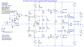
Here's a proof of concept of a high power non switching MOSFET amplifier I've designed a few years ago; the prototype showed about 0.0005% THD at 500W/4ohm. Still needs some work to be something pushing in a chassis (in particular for the pesky clipping behaviour) but is otherwise perfectly stable and doesn't do any really nasty things, like latching, when overloaded. Thanks to the non switching behavior it doesn't need much loop gain to get distortions down to 5ppm, this one has about 60dB at LF. Loop gain can be pushed much further in frequency, there are large stability margins, some two pole compensation could be used,
It's not a simple design, as expected performance has it's price. The trimpots are not really required (they set the output stage bias and balance the output) if the output MOSFETs are reasonably matched. Usually devices for the same tube are good enough (that's what I used and barely touched the trimpots from their mid position, to bring the output offset to zero)). Unity loop gain frequency can be pushed much further, there are large stability margins, some two pole compensation could be used, so there's a lot of further improvements, unfortunately I am swamped with work and other projects, so this one may wait until I will retire (few years to go).
I have somewhere the measurement results, I'll dig for if there's any interest.
Attachments
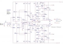

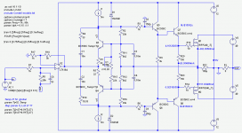
And here's a much simpler bipolar version; this one did not go beyond the simulation stage; it works fine in the computer, the distortion results @100W/8ohm are slightly worse than the version with MOSFETs.
Not my design, found it somewhere on the internet. I was looking for a smart compensation schema for it, beyond the rudimentary phase correction in the attached schematic, before trying to move it on the bench. Didn't find anything obvious/clear, Spice trial and error method is not something I enjoy doing, time was short, so I gave up. If somebody wants to pick up and make it a working amplifier worth of building, be my guest.
Not my design, found it somewhere on the internet. I was looking for a smart compensation schema for it, beyond the rudimentary phase correction in the attached schematic, before trying to move it on the bench. Didn't find anything obvious/clear, Spice trial and error method is not something I enjoy doing, time was short, so I gave up. If somebody wants to pick up and make it a working amplifier worth of building, be my guest.
Attachments

It is Cadence Capture/PSpice latest version, you won't be able to open it. Do everybody a favor and re-capture in LTSpice.
Last edited:
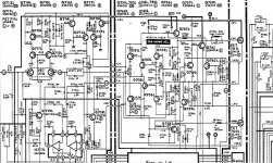
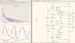
This belongs to a class of circuits that uses a small signal class AB stage to split the desired output current into two halves. Then, two separate current controlled current sources (cccs) amplify each half-wave, and the resulting current is summed at the output.
This entire circuit class does not work for several reasons:
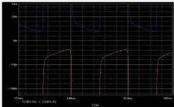
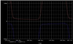
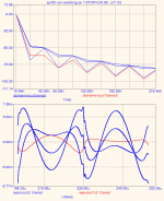
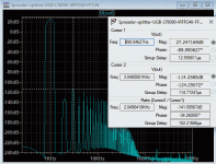
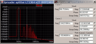
1) Even if the splitter is ideal and generates two half-waves whose sum is not distorted, for the same to happen at the output, both CCCS must have exactly the same gain at all frequencies. If they have 1% gain mismatch, then 1% of the halfwave current, which is almost entirely distortion with tons of high harmonics, will end up in the output. Attached simulations for various levels of mismatch, including no mismatch. It makes lots of high harmonics that don't fall off with frequency.
2) Each half, or top and bottom CCCS, processes a halfwave rectified version of the output current, which contains a lot more high frequency than the original signal. From these, each half will create its own intermodulation products, which will never match and will never cancel in the output.
This entire circuit class does not work for several reasons:
1) Even if the splitter is ideal and generates two half-waves whose sum is not distorted, for the same to happen at the output, both CCCS must have exactly the same gain at all frequencies. If they have 1% gain mismatch, then 1% of the halfwave current, which is almost entirely distortion with tons of high harmonics, will end up in the output. Attached simulations for various levels of mismatch, including no mismatch. It makes lots of high harmonics that don't fall off with frequency.
2) Each half, or top and bottom CCCS, processes a halfwave rectified version of the output current, which contains a lot more high frequency than the original signal. From these, each half will create its own intermodulation products, which will never match and will never cancel in the output.
Attachments
Doesn't work perfect, which is what you are after. Absolute perfection or absolute failure exist only in simulators.
I was looking forward to put this on the bench, but I could not make it stable to my satisfaction, in a sensible way.
The discrete version above works perfectly on the bench, with the indicated results (probably also not perfect to your criteria). As I said, it is rather complex though.
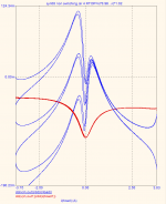
I remember for open loop (as you did above), the THD increases by some 20-25% with 10% imbalance (which can be easily compensated using the trimpots!) to a maximum of 0.5% (on the bench) with the most energy in the 2nd harmonic (probably due to the MOSFET output stage). No high order harmonics.
This approach is obviously inferior to the geometric collector/drain currents approach used by the LT1166 and that Edmond tried to simulate (which I believe is the best strategy) - unfortunately I still have to see an implementation that works properly.
I was looking forward to put this on the bench, but I could not make it stable to my satisfaction, in a sensible way.
The discrete version above works perfectly on the bench, with the indicated results (probably also not perfect to your criteria). As I said, it is rather complex though.
I remember for open loop (as you did above), the THD increases by some 20-25% with 10% imbalance (which can be easily compensated using the trimpots!) to a maximum of 0.5% (on the bench) with the most energy in the 2nd harmonic (probably due to the MOSFET output stage). No high order harmonics.
This approach is obviously inferior to the geometric collector/drain currents approach used by the LT1166 and that Edmond tried to simulate (which I believe is the best strategy) - unfortunately I still have to see an implementation that works properly.
Last edited:
It oscillated in simulation, the 2 ferrite beads in the CFP emitters fixed it. 3 transistor loop, that's trouble.
I'm not going after perfection, rather a good compromise.
I'm not going after perfection, rather a good compromise.
Hi Ovidiu, peufeu,And here's a much simpler bipolar version;...
Ovidiu, that second one is interesting how the splitting transistors are effectively bias spreaders as well. They don't give non-switching Class-AB by themselves but the 5k6 resistor across their collectors (R838) stops current turn off on one side.
Here is a circuit I have been looking at. It also uses the spreader transistors as splitters but NOT non-switching as I am using MOSFETs (but it can be made non-switching).
It's still in early stages of simulations.
I1 and I2 are temporary while I developed the main parts. C3 and C4 are set to 1F just for plotting the gain function at 1Hz -- they would normally be 10mF/6V, since the base node needs a very low impedance for a high internal gain (80dB at MF and LF).
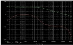
Peufeu, BTW R22 is not the same as source resistors for the MOSFETs, so it not an "evil source resistor". It provides some degeneration which reduces the compensation with R4,R10 which gives higher BW (20MHz small-signal) and less high-order harmonics at 1W. The closed loop bandwidth is 200kHz which is mainly due to the opamp and with C5 '3p3' it is over compensated just for better clip recovery.
Anyone running the circuit, for some reason it needs Alternate solver engine on LT-XVII.
Attachments
A relative of the last post with a normal voltage opamp by using an output stage with voltage gain.
THD is higher (1W 0.3ppm) and overall BW is higher (8 MHz).


.
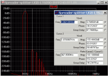
Although this and last post are not Auto Bias they allow a comparison to a conventional bias sensor -- to help decide whether an Auto Bias scheme is worth the extra effort. An Auto Bias has no thermal lag distortion while a conventional bias sensor does have TLD. An Auto Bias has no bias trimpot while a conventional bias sensor does have one.
THD is higher (1W 0.3ppm) and overall BW is higher (8 MHz).
.
Although this and last post are not Auto Bias they allow a comparison to a conventional bias sensor -- to help decide whether an Auto Bias scheme is worth the extra effort. An Auto Bias has no thermal lag distortion while a conventional bias sensor does have TLD. An Auto Bias has no bias trimpot while a conventional bias sensor does have one.
Attachments

- Home
- Amplifiers
- Solid State
- Towards a wideband non switching Auto Bias power amp