>C1/C11 are not needed[..]
Sorry, didn't see well. My post was regarding different case, not THESE C1/C11...
However you may still need different values for gate stoppers (upper vs. lower)
For the moment, I have 330R and 270R.
Hi Ricardo,
I've been tinkering with a similar design in simulations. Nothing in real life yet. Similar to your design but with a rush cascode for the feedback and a mu-follower for the load. These two added elements made a significant improvement in performance with a 2nd order dominate monotonically descending distortion profile. In addition, the use of a P type input device provides for negative phase 2nd order harmonics with minimal phase shift from 90 degrees (in simulations at least). This was my goal based on inspirations from Nelson Pass's research on the phase of harmonics.
Note: To achieve this I also used a single transistor VAS based on the the KSC1845 (not shown). This was needed to keep the phase shift to a minimum. The VAS is buffered to keep dissipation down.
The rush cascode is inspired by Juma's thread
25W Class A amp with Lateral MOSFETs. Specifically the design from post #180.
The Q5 is a LSJ689 to allow for rails to approach 50V (I simulated in the 38 to 45 range). Q3 is also a LSJ689, but this is just to make use of the other half. If could also be a BJT. I didn't seem any material differences in simulations.
The Mu follower does make setting the current through Q1 a bit tricky. The value needed for P1 can vary quite a bit with Idss of Q1 and Q3. I added Rsense as a way to measure it and allow P1 to be adjusted to a specific current. 1mA in this example. This current will impact DC offset. A value needs to be selected such that the Servo (or whatever mechanism you are using) has enough authority to address it.
The design looks promising in simulations and I have it on the to-do list to try and actually build it. I can share more details if anyone is interested, but don't want to highjack the thread from Ricardo.
Attachments
Good choice of gate stoppers but the caps act differently... they are there to avoid oscilations
An additional comment on my post and the use of a Rush cascode in the feedback loop. This does have a negative impact on damping factor. Something would likely need to be done to address this if this was used. Maybe positive current feedback similar to the F7?
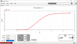
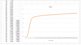
I used an atlas tracer to get the ccs response but the atlas does not go higher than 12V so I used a bench psu and got a better view when powering the ccs up to 43V.
Using 40V as reference...at 39V current is -0.35% lower and at 41V 0.33% higher... not very stiff but it works.
Thank you Mark for showing the way to use the curve tracer 🙂
Using 40V as reference...at 39V current is -0.35% lower and at 41V 0.33% higher... not very stiff but it works.
Thank you Mark for showing the way to use the curve tracer 🙂
Attachments
Interesting design. A couple of comments - the VAS pair have a rather low bias resistor of only 390 ohms. Given the emitter resistor of the VAS is 22 that limits the gain of the stage considerably.
Would be worth considering an active load (current mirror with the reference arm driven by the same current as in the FET). I've used that idea a long time ago and Kokoriantz did it for his version of the JLH 10W.
I recommend keeping the CCS for the input stage and VAS on separate bias chains, and not coupling them. In fact that separation should be done oin Self's Blameless too. Combining the two lends itself for modulating the VAS or input stage current by the other stage. Near clipping particularly, a single bias could disrupt the circuit. Self separated the VAS and input stage with a 1k resistor but that slows down the VAS transistor. Not recommended to combine the two diodes. Cost of a resistor and LED or so is a small expense for a hifi design.
Hi John
I did your proposed mod and indeed there is a substantial reduction in THD...
I am using a floating cascoded jfet ccs to feed the mirror.
Offset is set by R23 pot.
Very interesting concept thank you so much.
Attachments
Hi BrianThe design looks promising in simulations and I have it on the to-do list to try and actually build it. I can share more details if anyone is interested, but don't want to highjack the thread from Ricardo.
Thank you very much for your post.
Yours is an advanced design with concepts that I did not consider in my ultra simple design.
I do not think you are highjacking... not at all... If you wish you can elaborate a bit more here because I am eager to learn.
But right now what I really need is to know how to reduce offset fluctuations in my actual build.
My initial idea is using a matched pair of nfets for the IPS and IPS CCS, thermaly bonded.... but I also read that the major offset thermal variations might come from the VAS.... what do you think ?
As you are surely aware, with a singleton, DC offset doesn't naturally NULL. So a servo or some other means is needed to keep it in check.
In my simulations (not an actual build), I found DC offset was impacted by:
For #1, you could address this with a regulated supply for the IPS and VAS. Only worth pursing if you can mitigate the other items.
For #2, keeping the dissipation low by cascodes and/or heatsinking can mitigate this.
For #3, this is harder to address. In addition. it's hard to observe in an actual build, unless you have a way to actually run the device at different ambient temps.
For #4, The Idss range of JFETs can have a big impact. It's also tougher to simulate this. I've made crude attempts by tweaking some of the model parameters... just enough to see that the DC offset is materially impacted.
All of this led me to using a servo to control DC offset. I prefer your approach of a discrete solution. I believe Gareth Ingram (user Bigun) uses a similar approach in his TGM8 singleton design. However, I couldn't seem to get this approach to work in simulations. This does seem to be an approach many realized designs have used, so maybe this is a case where simulations and reality don't agree.
I'll post the design I've been working on later today. Along with notes on the challenges I don't have an answer for yet.
In my simulations (not an actual build), I found DC offset was impacted by:
- Power Supply Fluctuations
- Temperature changes between cold and hot states
- Ambient temperature fluctuations
- Variations in devices
For #1, you could address this with a regulated supply for the IPS and VAS. Only worth pursing if you can mitigate the other items.
For #2, keeping the dissipation low by cascodes and/or heatsinking can mitigate this.
For #3, this is harder to address. In addition. it's hard to observe in an actual build, unless you have a way to actually run the device at different ambient temps.
For #4, The Idss range of JFETs can have a big impact. It's also tougher to simulate this. I've made crude attempts by tweaking some of the model parameters... just enough to see that the DC offset is materially impacted.
All of this led me to using a servo to control DC offset. I prefer your approach of a discrete solution. I believe Gareth Ingram (user Bigun) uses a similar approach in his TGM8 singleton design. However, I couldn't seem to get this approach to work in simulations. This does seem to be an approach many realized designs have used, so maybe this is a case where simulations and reality don't agree.
I'll post the design I've been working on later today. Along with notes on the challenges I don't have an answer for yet.
Hi Brian
I built a variant of the TGM8 where I use the same offset control as Gareth did and it works wonderfully. In my build I have offset slow variations from 1 to 2mv.
But this time I used a different approach as I set the IPS jfet current using a CCS. In this case the offset varies more 1 to 12mV and the fluctuations are faster.
That is why I am trying to thermaly couple the new jfet ccs and the input device hoping this helps.
As you are surely aware, with a singleton, DC offset doesn't naturally NULL. So a servo or some other means is needed to keep it in check
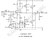
The Threshold NS10 preamplifier (designed by Nelson Pass in 1978) uses a singleton input, plus a DC servo to keep it in check. Schematic below. DC servo circuit includes the opamp at bottom left.
_
Attachments
Why use 2SK369? It is pretty hard to obtain ...
You can easily get LSK389 here:
DMOS Switches, JFET Amplifiers, BIFET Amplifiers, MOSFETS
I believe it is even better for this purpose as you can use one side for ips and the other for ccs.
Alternative: LSK489
In my build I am using LSK170BL
The Threshold NS10 preamplifier (designed by Nelson Pass in 1978) uses a singleton input, plus a DC servo to keep it in check. Schematic below. DC servo circuit includes the opamp at bottom left.
_
Yes... but he uses an input cap...
Using an input cap I could easily implement a biasing scheme like the one I am using here:
HDRP200 High speed very low distortion singleton power amplifier
It works very well but this time I do not want an input cap.
Today I changed again the compensation...
1st build miller 33p sounded super detailed in the bass but I noticed some stress in cymbals and slight brightness in trompetes.
2nd mod 43p miller, cured any brightness but bass lacked a bit of snap.
3rd mod miller 33p and c15 from vas collector to fb node is now 10p..... the best compromise yet.... bass has snap and no edginess in the tremble. Will let it sing like that for a while
My first impressions are very positive....
The bass is very detailed and snappy and now I can hear trompetes and violins at high volumes without any nasties.
I noticed an evident change in tone... acoustic guitar has a slight wood sound prominence so this technique must be used carefully.
Also there is a slight increase in 2nd harmonic... good for some old recordings.
I measured the amp with arta and the harmonic distribution is monotonic... 2>3>4>5>6>7
And i can hear the typical k170BL sound.... very good.
As for offset, it starts at -0.3V and goes down to 30mv after 10 minutes.... not bad.
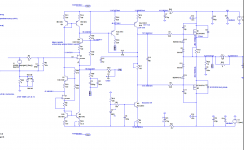
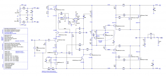
Here's the design I mentioned in post #23. It only exists in simulations 🙁. In this imaginary state, it achieves predominately 2nd order negative phase harmonics (The attached LTSpice error log is 1W into 8Ω at 1kHz)
In real-life, I image it could be a bit tricky to stabilize. It uses a two pair CFP lateral mosfet output stage without emitter resistors. Even with the use of lateral mosfets, the lack of emitter resistors makes the bias settings unstable with a conventional single transistor bias network. Therefore, it uses a CFP bias network. The design is borrowed from user Bonsai's NX amplifiers. With this arrangement, it seems to be much more tolerant of power supply and temperature fluctuations.
To set the bias, you'll need a power supply with a CRC arrangement. Measure the current across the "R" in the CRC of the power supply. Then back out the current across R29/R30 to get the OPS bias current. This assumes the pairs would be Exicon's matched ECX10N20-S / ECX10P20-S devices.
The compensation is Miller Input Compensation (as Bob Cordell refers to it). C3 adds a bit of lead compensation
Q3 is the Mu-follower for the active load on Q1. P1 allows you to set the IPS current which will otherwise vary due to the range of Idss values possible between Q1 and Q3.
Q13 is a driven cascode. When auditioning in real-life, I'd probably want to tinker with removing R10 to see if a cascode vs driven cascode makes any sonic differences.
Q4 is the VAS and Q5 is the buffer since Q4 is only a TO-92 device. This keeps the dissipation in Q4 more manageable. I opted for this arrangement to allow for use of a single device Low Cob transistor. This keeps the overall harmonics predominately 2nd order with minimal phase shift from 90 degrees. I don't know how much this actually matters - but it was the goal of this design after reading a lot of Nelson Pass articles and posts on the phase of harmonics.
I mentioned in post #25 that it had a problem with output impedance. This was an error on my part... forgot to ground the input.
DC Offset is managed with a servo. You could also try a discrete solution without an opamp. Though in simulations, it didn't seem to keep DC nulled when ambient temperature changes were introduced.
Hopefully I'll get around to building it one of these days to see if it actually works 🙂. Which means the Ricardo's design is much better because he's actual build it
I've attached the LTSpice files if anyone whats to tinker with it.
Attachments
Ultra low distortion wasn't the goal. I doubt anyone tinkering with singleton IPS topologies is striving for that. There's plenty of other designs out there that accomplish that.
Thank you Brian
You have really pushed the singleton idea to a new (higher) level.
Food for the mind it is.... will take me a while to grasp all the concepts but for now I already like the servo layout although the injection resistor R92 seems to small....
You have really pushed the singleton idea to a new (higher) level.
Food for the mind it is.... will take me a while to grasp all the concepts but for now I already like the servo layout although the injection resistor R92 seems to small....
- Home
- Amplifiers
- Solid State
- Singleton Jfet Input with laterals.... very fast amp