Looking for a good power amplifier, I initially designed and built a "LIN" amp with cascoded jfet input, "buffered TIS", high current drivers and Lateral mosfets outputs that I have been using as my main system amp.
I grew used to its unparalleled low distortion, sheer bass slam and overall musicality.
Then I designed and built a smaller amp with singleton IPS, bootstrapped TIS, ccs mirror loaded resistor as driver and lateral outputs.
This one did not have the same "slam factor" but had some major virtues like improved voice presentation, and much increased microdetail rendering when compared with the LIN amp.
I wanted to have the best of both worlds so I started designing a new very low noise / low distortion singleton.
This time I decided to go the "less is more" way in order to boost clarity without impairing other sonic factors.
1 – Input Stage (IPS)
I am using a single NPN for the input stage.
I chose the KSC1845 with high hFe, able to stand the high rail voltages needed for a 200W amplifier, with very low Cob (does not need cascoding) and a high fT 110MHz.
To minimize noise, I chose to run it at low standing current (0.5mA).
To increase gain the NPN collector is CCS loaded, I designed a CCS able to work with very low In-Out voltage drop.
The collector current drives the TIS that converts it into voltage swing.
The biasing is very simple and I added a second KSC1845 connected as a diode (base to collector shorted) in the circuit to control voltage drift due to temp changes. This transdiode is thermally coupled to the input transistor in my build.
2 – Transimpedance stage (TIS)
The TIS (VAS) is built with two transistors:
The first one is connected as an emitter follower (beta enhancer) that drives the second one acting as the proper TIS.
Miller compensation is set around these two transistors.
The beta enhancer is a BC556B chosen for its very high speed (280Mhz), low Cob (3pF) and high hFe.
The TIS is a 2SA1381 a medium power PNP with outstanding characteristics. It withstands high voltages (300v), high speed (fT 150Mhz) and very low Cob (3pF).
I needed a medium power PNP because I am using it to drive the lateral output mosfets directly (without drivers).
After long discussions with some experts, I now know that lateral mosfets basically need enough current to charge its input capacitance but it is not fundamental to have a low output impedance driver as these mosfets have very high input impedance.
To have the “natural voice rendering” I decided to bootstrap the TIS but to have the fundamental “bass snap” I used a floating depletion mode mosfet CCS as the upper resistor in this bootstrap. (Here I had the guidance from Hugh Dean and also followed Damir’s information gathered here: bootstrapsCCS+T-TMC)
3 - Miller compensation
As I wanted to use a small value for the miller capacitor, I included another capacitor in parallel with the series feedback resistor in order to increase phase margin.
4 – Output Stage (OPS)
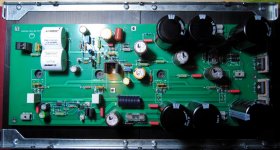
For the outputs I chose the double dye laterals from exicon that are designed for 250W each so I could get away with only two pairs, saving precious board space, having larger distances between them for ease of heat dissipation and still being able to design for 200W into 8 ohms.
Biasing these mosfets is done with a resistor fed directly from the TIS.
The amp is terminated with the usual Zobel included to make sure the output sees a resistive load at high frequencies, keeping the open loop gain in control.
The output inductor is there to guarantee the load going inductive at HF. If we drive (long) cables, certain filter topologies, or a piezo tweeter, the load doesn't turn inductive at high frequencies, but capacitive. Here, the Zobel scheme does not work, so I included a series inductor in the amplifier to avoid oscillations.
The resistor parallel to the L is there because a series-resonance circuit is formed by the combination of the output inductor and a capacitive load, which forms a short at resonance. The resistor in parallel with the inductor reduces the Q of this circuit, preventing the short from occurring.
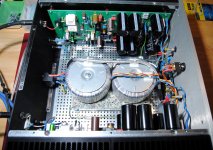
To increase image rendering I built the prototype in dual mono style with one transformer for each channel.
Each transformer has two secondaries that feed one bridge each.
Rectifying and smoothing circuits are included in the amps board so the reservoir caps are near the demanding output devices.
Local decoupling caps are provided and all gnd return paths are independent in the pcb layout.
Capacitor bank size was determined based on the splendid spreadsheet from Thomas P. Gootee.
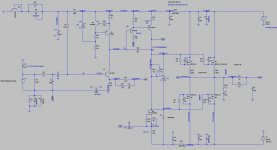
I used LT-Spice to simulate the design before the build and will provide here some asc files so everyone can also play with it.
Ricardo Cruz
I grew used to its unparalleled low distortion, sheer bass slam and overall musicality.
Then I designed and built a smaller amp with singleton IPS, bootstrapped TIS, ccs mirror loaded resistor as driver and lateral outputs.
This one did not have the same "slam factor" but had some major virtues like improved voice presentation, and much increased microdetail rendering when compared with the LIN amp.
I wanted to have the best of both worlds so I started designing a new very low noise / low distortion singleton.
This time I decided to go the "less is more" way in order to boost clarity without impairing other sonic factors.
1 – Input Stage (IPS)
I am using a single NPN for the input stage.
I chose the KSC1845 with high hFe, able to stand the high rail voltages needed for a 200W amplifier, with very low Cob (does not need cascoding) and a high fT 110MHz.
To minimize noise, I chose to run it at low standing current (0.5mA).
To increase gain the NPN collector is CCS loaded, I designed a CCS able to work with very low In-Out voltage drop.
The collector current drives the TIS that converts it into voltage swing.
The biasing is very simple and I added a second KSC1845 connected as a diode (base to collector shorted) in the circuit to control voltage drift due to temp changes. This transdiode is thermally coupled to the input transistor in my build.
2 – Transimpedance stage (TIS)
The TIS (VAS) is built with two transistors:
The first one is connected as an emitter follower (beta enhancer) that drives the second one acting as the proper TIS.
Miller compensation is set around these two transistors.
The beta enhancer is a BC556B chosen for its very high speed (280Mhz), low Cob (3pF) and high hFe.
The TIS is a 2SA1381 a medium power PNP with outstanding characteristics. It withstands high voltages (300v), high speed (fT 150Mhz) and very low Cob (3pF).
I needed a medium power PNP because I am using it to drive the lateral output mosfets directly (without drivers).
After long discussions with some experts, I now know that lateral mosfets basically need enough current to charge its input capacitance but it is not fundamental to have a low output impedance driver as these mosfets have very high input impedance.
To have the “natural voice rendering” I decided to bootstrap the TIS but to have the fundamental “bass snap” I used a floating depletion mode mosfet CCS as the upper resistor in this bootstrap. (Here I had the guidance from Hugh Dean and also followed Damir’s information gathered here: bootstrapsCCS+T-TMC)
3 - Miller compensation
As I wanted to use a small value for the miller capacitor, I included another capacitor in parallel with the series feedback resistor in order to increase phase margin.
4 – Output Stage (OPS)
For the outputs I chose the double dye laterals from exicon that are designed for 250W each so I could get away with only two pairs, saving precious board space, having larger distances between them for ease of heat dissipation and still being able to design for 200W into 8 ohms.
Biasing these mosfets is done with a resistor fed directly from the TIS.
The amp is terminated with the usual Zobel included to make sure the output sees a resistive load at high frequencies, keeping the open loop gain in control.
The output inductor is there to guarantee the load going inductive at HF. If we drive (long) cables, certain filter topologies, or a piezo tweeter, the load doesn't turn inductive at high frequencies, but capacitive. Here, the Zobel scheme does not work, so I included a series inductor in the amplifier to avoid oscillations.
The resistor parallel to the L is there because a series-resonance circuit is formed by the combination of the output inductor and a capacitive load, which forms a short at resonance. The resistor in parallel with the inductor reduces the Q of this circuit, preventing the short from occurring.
To increase image rendering I built the prototype in dual mono style with one transformer for each channel.
Each transformer has two secondaries that feed one bridge each.
Rectifying and smoothing circuits are included in the amps board so the reservoir caps are near the demanding output devices.
Local decoupling caps are provided and all gnd return paths are independent in the pcb layout.
Capacitor bank size was determined based on the splendid spreadsheet from Thomas P. Gootee.
I used LT-Spice to simulate the design before the build and will provide here some asc files so everyone can also play with it.
Ricardo Cruz
Attachments
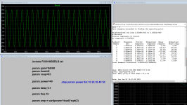
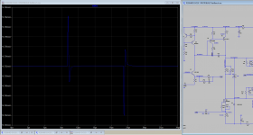
FFT @ 40W shows 0.000312% THD
To play with this sim you can change output power:
.param power=40
And frequency:
.param freq 1k
To have consistent values from the FFT graph and error log I suggest:
.param delay 0.1 for 1khz
.param delay 0.01 for 20khz
To play with this sim you can change output power:
.param power=40
And frequency:
.param freq 1k
To have consistent values from the FFT graph and error log I suggest:
.param delay 0.1 for 1khz
.param delay 0.01 for 20khz
Attachments
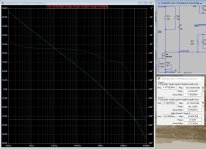
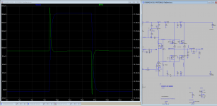
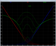
CLG and OLG showing linear response with -3dB @ 466khz
Notice OLG 100dB until 1khz
Notice OLG 100dB until 1khz
Attachments
Last edited:
Nice project.
From the picture you seem to have already completed the project but you state data form virtual analyser?🙄
This reminds me a bit of the Fetzilla amplifier but you have mainly replaced the jfet input stage with bjts and used also bjt as TIS ( VAS).
Fetzilla Build Documentation
Have you got the chance to compare both amplifiers for difference in sound?
If you are matching the output mosfet you could get rid of the source resistors and increase the class A operation. You can still use a very small value (0.02 ohms for example) to allow ease of bias current measurement.
Thanks for sharing.
Fab
Last edited:
Fab
Thank you for your comments.
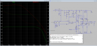
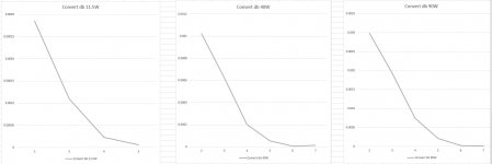
I did a FFT analysis of the built amp using visual analyser. I placed the measurements in a spreadsheet so I could visualize the harmonic distribution.
I did not know about the Fetzilla but this project has been discussed with Hugh Dean for a long time (first simulations where done in August 2020 ).... I see now the solutions he proposed where already implemented in his fet amp.
I initially built the HDRP200 with a "normal" bootstrapped TIS and althou the sound was incredibly detailed it did have a "too mellow" bass.
Hugh suggested replacing the upper bootstrap resistor with a floating ccs and that worked very well.
Source resistors where included to reduce transconductance droop at high currents.
I use source resistors on the positive side only to reduce crossover distortion by improving transconductance match of N and P devices.
This effectively reduces class A operation at low power levels but reduces crossover distortion at high output volumes.
To determine the value of this resistors I used a wingspread that helps to visualize the effect.
Thank you for your comments.
I did a FFT analysis of the built amp using visual analyser. I placed the measurements in a spreadsheet so I could visualize the harmonic distribution.
I did not know about the Fetzilla but this project has been discussed with Hugh Dean for a long time (first simulations where done in August 2020 ).... I see now the solutions he proposed where already implemented in his fet amp.
I initially built the HDRP200 with a "normal" bootstrapped TIS and althou the sound was incredibly detailed it did have a "too mellow" bass.
Hugh suggested replacing the upper bootstrap resistor with a floating ccs and that worked very well.
Source resistors where included to reduce transconductance droop at high currents.
I use source resistors on the positive side only to reduce crossover distortion by improving transconductance match of N and P devices.
This effectively reduces class A operation at low power levels but reduces crossover distortion at high output volumes.
To determine the value of this resistors I used a wingspread that helps to visualize the effect.
Attachments
I initially built the HDRP200 with a "normal" bootstrapped TIS and althou the sound was incredibly detailed it did have a "too mellow" bass.
Hugh suggested replacing the upper bootstrap resistor with a floating ccs and that worked very well.
I thik I was first to use combination of boostrap with floating CCS, I hope Hugh mentioned it.
bootstrapsCCS+T-TMC
Damir

I thik I was first to use combination of boostrap with floating CCS, I hope Hugh mentioned it.
bootstrapsCCS+T-TMC
Damir
Hi Damir
I did mention it in my first post.
Did you verify the sonic effect of the bootstrap capacitor in your build ?
I have seen values ranging from 47u to 470u but simulation does not differentiate between them (THD does not change).
I started with 220u but increased it to 330u and bass is clearer this way... what should I look for ?
Sorry I was to lazy to read your long text.😱
Higher cap value influence low frequency, simulate with 20Hz.
I built that amp long time ago, can't remember now, old age.🙁
BR Damir
Damir,
I was advised about the FetZilla bootstrap by a local EE who regrettably did not reveal it had come from you!!
I now acknowledge your idea formally here.
Thank you for your clever idea, and thanks to Ricardo for his exhaustive description of his new amp.
Ciao,
Hugh
I was advised about the FetZilla bootstrap by a local EE who regrettably did not reveal it had come from you!!
I now acknowledge your idea formally here.
Thank you for your clever idea, and thanks to Ricardo for his exhaustive description of his new amp.
Ciao,
Hugh
Unplug a speaker and the input of the other channel and listen, you must hear the music. The ground circuit breaker 5 ohm resistor links the two feedbacks. You must add a grounding resistor after the 1k R3 to balance. On simulator apply a voltage generator between earth and signal ground to simulate the voltage on the emitter of the input stage of the other channel, along with 68 ohm and 2200uF capacitor and see the ac analysis to adjust the balancing resistor.
Last edited:
You would put an emitter OE repeater at the input .Yes, the first cascade in the cascode would have been done.It would be a good idea.
Unplug a speaker and the input of the other channel and listen, you must hear the music. The ground circuit breaker 5 ohm resistor links the two feedbacks. You must add a grounding resistor after the 1k R3 to balance. On simulator apply a voltage generator between earth and signal ground to simulate the voltage on the emitter of the input stage of the other channel, along with 68 ohm and 2200uF capacitor and see the ac analysis to adjust the balancing resistor.
The 5ohm (R2) resistor is there only for simulation purposes..... in my build I left only the two diodes for protection so crosstalk is minimized.
I will try your idea and report here the results.
You would put an emitter OE repeater at the input .Yes, the first cascade in the cascode would have been done.It would be a good idea.
Please explain.....
- Home
- Amplifiers
- Solid State
- HDRP200 High speed very low distortion singleton power amplifier