Please explain.....
Here please
Attachments
hey Ricardo,
You have a very nice design, I love how you decided to use a common emitter stage loaded with a CCS to keep the even harmonics as part of the IPS's sound signature.
Have you tried to cascode DN2540 with a low noise Jfet?
I used DN2540 a lot in my tube gear and I have noticed that by itself it does not make a good sounding CCS.
Some links that could be useful:
CCS: not everything that glitters is gold (Part I) – Bartola(R) Valves
Mini CCS – Bartola(R) Valves
Flexible CCS board prototype – Bartola(R) Valves
Tracing (MOS)FETs to be used in the gyrator PCB – Bartola(R) Valves
Best regards,
Silviu Savu
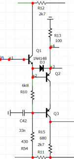
The 5ohm (R2) resistor is there only for simulation purposes..... in my build I left only the two diodes for protection so crosstalk is minimized.
I will try your idea and report here the results.
Without 5 ohms is worst.
The 5ohm (R2) resistor is there only for simulation purposes..... in my build I left only the two diodes for protection so crosstalk is minimized.
I will try your idea and report here the results.
Without 5 ohms is worst.
Please excuse me, R2 must remain in place as it is the GND lift for the IPS.
Here please
Thank you for your comment.
Would you care to mod my asc file so I can follow what you mean ?
hey Ricardo,
You have a very nice design, I love how you decided to use a common emitter stage loaded with a CCS to keep the even harmonics as part of the IPS's sound signature.
Have you tried to cascode DN2540 with a low noise Jfet?
I used DN2540 a lot in my tube gear and I have noticed that by itself it does not make a good sounding CCS.
Some links that could be useful:
CCS: not everything that glitters is gold (Part I) – Bartola(R) Valves
Mini CCS – Bartola(R) Valves
Flexible CCS board prototype – Bartola(R) Valves
Tracing (MOS)FETs to be used in the gyrator PCB – Bartola(R) Valves
Best regards,
Silviu Savu
I did simulate a cascoded CCS but was unsure of the resulting current stability.
Would you please suggest a suitable jfet for this purpose ?
Thank you for your comment.
Would you care to mod my asc file so I can follow what you mean ?
I don't work in LTC spice.I can't change it.
Circuit description:
IPS
Q1 – KSC1845 NPN – Input transistor running @ 540uA
IPS CCS
Q5 – BC560C PNP (Controlling bjt)
Q4 – BC560C PNP (Stiff bjt)
R29 – 100 ohm (Base stopper to avoid instability in the CCS)
R28 – 1k2 ohm (Current setting resistor)
R27 – 15kohm + R32 – 15kohm (current setting resistors for the CCS controlling bjt)
C21 – 47u (Filter for R27 R32 current setting resistors for the CCS controlling bjt)
IPS BIAS
R5 – 32k4 ohm + R31 – 2kohm // 1k trimmer (voltage divider provides base bias voltage for Q1)
R4 – 32k4 ohm (voltage injector – places Bias on Q1 base)
C3 – 470u (Bias circuit filer / stabiliser)
Q7 – KSC1845 NPN (connected as a transdiode “base collector shorted” is there for anti drift purposes as it is thermally bonded to Q1)
TIS (VAS)
Q2 – BC556B PNP (Beta helper… this EF shields the TIS transistor increasing the circuit input impedance and total beta)
Q3 – 2SA1381C PNP (TIS transistor provides current to voltage conversion)
C24 – 25pF (Miller compensation capacitor ” CDOM ”)
R11 – 11 ohm (TIS emitter degeneration)
R10 – 220 ohm (beta helper emitter resistor)
R12 – 12k ohm (power limiter for the beta helper bjt)
TIS CCS Boostrap
R15 – 1k5 ohm (-Rail boostrap resistor)
C7 – 330uF (Bootstrap capacitor connected to the output)
M5 – DN2540 (N-Channel Depletion-Mode Vertical DMOS FET connected as floating CCS)
R34 – 330 ohm (base stopper for DN2540)
R24 – 82 ohm (sets the CCS current used as TIS idling)
OPS
M1 – M2 – Lateral NMOS ECW20N20-S
M2 – M4 – Lateral PMOS ECW20P20-S
R17 – R18 – 270 ohm (NMOS gate stopper)
R19 – R20 – 180 ohm (PMOS gate stopper)
R25 – R26 – 0.2 ohm (NMOS emitter resistor)
OPS BIAS
R13 – 120 ohm // R30 – 1kohm trimmer (uses TIS standing current to set bias on the output lateral mosfets)
C9 – 47u (helps turnoff output devices)
FEEDBACK Circuit
R8 – 1k8 ohm (series feedback resistor)
R9 – 68 ohm (shunt feedback resistor)
R33 – 100 ohm (shields Q1 emitter from the action of C4)
C4 - 22pF (Lead compensation capacitor)
C5 – 2200uF (nuls feddback at DC so Gain is unity at DC)
INPUT CIRCUIT
C14 – 22nF (connected between signal GND and chassis, filters input RCA and lowers sensitivity to EMI)
R1 – 220k ohm (input RCA load)
R3 – 1k ohm (input low pass filer set to 720kHz with C2)
C2 – 220pF (input low pass filter)
C1 – 10uF (Input DC blocking capacitor)
R2 – 5 ohm (lifts signal GND from power supply GND reducing hum)
D7 – D8 – 1N4148 (closes circuit around R2 for high current protection in case of fault)
MOSFET GATE PROTECTION
D1 – MURS320 (Clamps the bootstrap and so limits output devices Gate Source voltage to below 4 volts in case of overvoltage at the input)
Attachments

I don't work in LTC spice.I can't change it.
Can you print one of my schematics, draw you correction over it and post here a picture please ?
Is it difficult to log in to one repeater? The collector and emitter on the power bus to lean and all.You don't need a cascode.
I did simulate a cascoded CCS but was unsure of the resulting current stability.
Would you please suggest a suitable jfet for this purpose ?
Well in depends on how much current you run trough the CCS. I did not get to run your simulation yet... But the jfet has to withstand the VAS current.
Is it difficult to log in to one repeater? The collector and emitter on the power bus to lean and all.You don't need a cascode.
What is the repeater ?
I am not using any cascode.
Please elaborate.
Are you referring to the ips ccs?
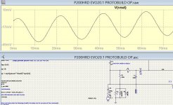
The ac analysis goes wrong. I can sim the input stage on Tina if you want because the crosstalk is dependent on frequency, 10u, 2200u might need to be adjusted.
The 22nF from RCA shield..... is wired on the input.
The 22nF from RCA shield..... is wired on the input.
Attachments
Last edited:
Yes, my error, the 22nF is connected between the RCA gnd and the chassis.
I posted a corrected schematic in post 29
I posted a corrected schematic in post 29
I made the 5 transistor version with LF353 servo 25 years ago for car stereo.
performance is excellent until it clips, then the rails stick noticeably.
Mine was all reverse transistors, 2N5401 x2 2N5551x 1 and IRF530 , IRF9530.
PNP vas versus NPN vas may be better
performance is excellent until it clips, then the rails stick noticeably.
Mine was all reverse transistors, 2N5401 x2 2N5551x 1 and IRF530 , IRF9530.
PNP vas versus NPN vas may be better
- Home
- Amplifiers
- Solid State
- HDRP200 High speed very low distortion singleton power amplifier