Inspired by brilliant shine of Blowtorch four-quadrant self-biased input stage and trying to build something bridged we need to control output common mode.
This is the one more or less simple approach, based on the current summing of two nodes. First loop are controlled by input signal, while second are controlled by output common mode.
This is the one more or less simple approach, based on the current summing of two nodes. First loop are controlled by input signal, while second are controlled by output common mode.
Attachments
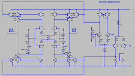
Correcting the common mode is done on both upper or lower current mirrors, by injecting the amplified residual sum of both outputs. However, the 'sides' on the CM's up and down may respond different from the CM-control outputs. Q21 and Q22 are not responding exactly the same, and will not be compensated (completely) by Q23 and Q24, having their own affairs. The results will be two not related dc components on the outputs, being the state of equilibrium. If everything is ok with that, modulating the inputs might proove to become even more challanging for the CM-control circuitry.
There is always some risks with double feedbackloops.
There is always some risks with double feedbackloops.
Last edited:
Not clearly the sum, it's better to say centertap of the difference to ground.Correcting the common mode is done on both upper or lower current mirrors, by injecting the amplified residual sum of both outputs.
being the state of equilibrium.
Any fully-differential topology is a kind of equilibrium since have no fundamental reference and must synthesise signal reference by itself.
Clearly!There is always some risks with double feedbackloops.
So, for that topology it's better to use high intrinsic CMRR input stage to reject common mode noise from the input and internal common-mode loop can work mostly in low-frequency range for keeping amp's shoulders in the center of supply rails.
Ok, well, the whole core could be redrawn to folded cascode topology and common mode loop can be injected in upper current sources, so excluding push-pull mode.Q21 and Q22 are not responding exactly the same
I am assuming that this circuit is incomplete, no compensation is shown...
Clearly!
Thats a core concept based on two main ideas:
1. Currents could be simply summed at emitters of common base VAS input node or even with common emitter VAS just be injected in the emitter.
2.VAS node anyway have two inputs - base and emitter with slightly different kind of reaction, but anyway we can use them both for summing different loops reaction.
Since we're already differential and thus inverting the main compensation could be external like this:
https://www.diyaudio.com/forums/solid-state/320727-opamp-common-base.html#post5435606
Last edited:
That's an academic rephrase. As you like it.Not clearly the sum, it's better to say centertap of the difference to ground.
Ditto. Agreed.Any fully-differential topology is a kind of equilibrium since have no fundamental reference and must synthesise signal reference by itself.
If so it becomes a quadrature control loop, no more easy alas....use them both...
In general, this topology uses the non-inverting gain stages with inescapable control and compensation circuitry. Inverting gain stages are in such a setup far more simpler to realise and don't need elaborate control loops. The only disadvantage is the low input impedance. If some serious amplification is needed with at least 10k inp-imp, a feedback network would become a crazy high Z, rendering it in a short wave radio receiver.
Oh no!!!! THS4131!!!! I designed the ADA4932, ADA4950, AD8475 and AD8476 which were competitors that part in some way...
Now, looking at your circuit, first glance there are a two things I do not like.
Assuming that there will be a second gain stage following each output of your circuit (so far you are showing a differential GM cell):
1. Your common mode circuit will be difficult to compensate since it is already has a HiZ node (collector of Q4 and collector of Q7).
2. The collector bias current of Q21-Q24 is undefined.
Also missing are degeneration resistors in your signal current mirrors, but I guess you know that and just have not placed them.
Bottomline, as is, I don't this circuit will work... still needs to be refined more.
Maybe, would need to see a schematic.
Best, Sandro
Now, looking at your circuit, first glance there are a two things I do not like.
Assuming that there will be a second gain stage following each output of your circuit (so far you are showing a differential GM cell):
1. Your common mode circuit will be difficult to compensate since it is already has a HiZ node (collector of Q4 and collector of Q7).
2. The collector bias current of Q21-Q24 is undefined.
Also missing are degeneration resistors in your signal current mirrors, but I guess you know that and just have not placed them.
Bottomline, as is, I don't this circuit will work... still needs to be refined more.
Thats a core concept based on two main ideas:
1. Currents could be simply summed at emitters of common base VAS input node or even with common emitter VAS just be injected in the emitter.
2. VAS node anyway have two inputs - base and emitter with slightly different kind of reaction, but anyway we can use them both for summing different loops reaction.
Maybe, would need to see a schematic.
Best, Sandro
If some serious amplification is needed with at least 10k inp-imp, a feedback network would become a crazy high Z, rendering it in a short wave radio receiver.
You can use low RG to keep RF low, and drive it with a dual op-amp.
I assume RG is the input resistor of the inverting amp? If so, that dual opamp in front is an extra amplifier in series with the amp itself, so how to fold them together? I've tried a T-network feedback, but it prooves very unstable in hf.You can use low RG to keep RF low, and drive it with a dual op-amp.
Agreed with your post #6 and points HiZ and corresponding node definitions.
Yes.I assume RG is the input resistor of the inverting amp?
Yes.If so, that dual opamp in front is an extra amplifier in series with the amp itself
Not sure what you mean. Attached is the schematic of what I am proposing. You technically do not need the 2nd op-amp, but it adds symmetry.so how to fold them together? I've tried a T-network feedback, but it prooves very unstable in hf.
Best, Sandro
Attachments
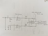
That's more or less the same I have in mind with a double inverting symmetrical bridge (triggered by BesPav initial contribution #1; sorry, we're not intentionally hijacking your topic currently) I'm working on some time now.Not sure what you mean. Attached is the schematic of what I am proposing. You technically do not need the 2nd op-amp, but it adds symmetry.
Other then BesPav noninverting circuit bridge, this setup is indifferent to the following and end stage configurations and needs no adjustments, control loops (intrinsic stable) or compensations during simulations (dc-100M); real life will force hf caps in the feedback though (parallel over Rf and Rg). But I want to get rid of the Az stage, which serve as impedance buffer only when I want Ri and Ro at low values (100Ω), keeping Rf and Rg at 1kΩ and comp-caps at sensible values. A T-network for Rf and Rg yields hf instability. There is no need for a second pre to buffer the ground node, not even in open loop!
However, Az can be a srpp or a single stage Pass pre amp (sounds obvious) or the like. Even more, like BesPav bridge design, there is way less stress on the power rails and dynamic demands.
Attachments
I assume RG is the input resistor of the inverting amp?
You can put an instrumentation opamp pair in front of fully-differential one.
Since CMRR more like than ∆R/R it's effective to increase input impedance higher than usual 10k.
Also ground wire needs to be the same impedance than the signal wire if an output filter on the source side is used.
Last edited:
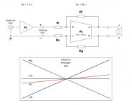
A closed loop. I truncate a lot.What is Ac?
Ao is A open loop.
Rf is feedback (regular), Rg is ditto (conduct), Ri is input (regular), Ro is zeroing reference. Az is impedance amplifier.
So far, with an actual circuit, I found no odd things during simulations (op, dc, ac, trans). Extremely boring results.
Oh no!!!! THS4131!!!! I designed the...
Oh, Sandro, i've just checked for your profile. Thank you for your input.
Yes, somthing like 4131 or even an AD797 (if it were fully-differential) can be simply build on a DIY manner. Of course with emitter degeneration.
Assuming that there will be a second gain stage following each output of your circuit
Yes, there could be one, or two, or even three gain stages, based on desired feedback depth and freq compensation.
But we're at the DIY territory, so i suppose even around 60 dB of feedback depth around fast enough OPS will be enough for pretty good THD figures. Also i'll prefer to degenerate as possible and highly load Hi-Z node for excluding the need of miller-like compensation. Let the core to be very fast in rise speed.
1. Your common mode circuit will be difficult to compensate since it is already has a HiZ node (collector of Q4 and collector of Q7).
Can be simply changed to straight current mirror from grounded LTP shoulder.
It anyway will have relatively high-z input, say some kOhms, so needed filtering or freq band can be designed at the common-mode loop input.
2. The collector bias current of Q21-Q24 is undefined.
Since it's signal picked from current-mirror loaded LTP it must be defined by LTP's source?
All true and agreed. But I want a very low Ri (most pre cannot drive), almost current driven. A high Ri and Ro needs that crazy high Rf and Rg, even parasitic capacitances brings the Fo... bandwidth back under 100k, so phase is running away from 10k already. Compensating within the bridge to overcome this (peaking) yields extreme sensivity to hf noise. A small build made mumbling voices and afar lighing audiable (on headphones).You can put an instrumentation opamp pair in front of fully-differential one.
Since CMRR more like than ∆R/R it's effective to increase input impedance higher than usual 10k.
Also ground wire needs to be the same impedance than the signal wire if an output filter on the source side is used.
Actually, both your and my bridge are children of instumentation opamps.
An instrumentation opamp to drive an instrumentation amplifier. Hmm...
Last edited:
Hi BesPav,
Can be simply changed to straight current mirror from grounded LTP shoulder.
That will work.
Since it's signal picked from current-mirror loaded LTP it must be defined by LTP's source?
Yes, the CM circuit LTP source.
If you send me your .asc file, I can do some tweaks. Just post it.
Now, my shameless plug , take a look at my for fun project (and share it with your friends):
SW Audio
It is my youtube channel on audio amplifier design fundamentals") .
.
Can be simply changed to straight current mirror from grounded LTP shoulder.
That will work.
Since it's signal picked from current-mirror loaded LTP it must be defined by LTP's source?
Yes, the CM circuit LTP source.
If you send me your .asc file, I can do some tweaks. Just post it.
Now, my shameless plug
, take a look at my for fun project (and share it with your friends):SW Audio
It is my youtube channel on audio amplifier design fundamentals
.But I want a very low Ri (most pre cannot drive), almost current driven.
Why not...
Common base or mirrored open emitter as input.
5 leg of AD844 at the source side as voltage-controlled current source (just load noninverting input to ground with gain resistance and feed your voltage to inverting leg, perfect V->I converter with at least 3 zero THD) and inverting AD844 leg as receiver, again with noninverting input feeded with 1-stage gain resistance to GNG and 5 leg to GND as 2-stage gain.
Hi-Z source and Lo-Z receiver as true current signal transfer.
Last edited:

- Status
- This old topic is closed. If you want to reopen this topic, contact a moderator using the "Report Post" button.
- Home
- Amplifiers
- Solid State
- Bridged topology with common-mode control