If you are looking for a diff in diff out amp (bridget) using a jfet frontend you could use something like I designed and put up many years ago.
It's a simplified schematic.
Stein
It's a simplified schematic.
Stein
Thanks. A bit hard to find the proper contribution. Can you share the # in that thread you're refering to?
Attached!If you send me your .asc file, I can do some tweaks. Just post it.
Certainly!take a look at my for fun project
Attached!Dear BesPav, please do draw me a sketch of it!
If you are looking for a diff in diff out amp (bridget) using a jfet frontend you could use something like I designed and put up many years ago.
Good input, thank you!
Some thoughts
1. input PN-junction aren't inside feedback loop, so can be a distortion source.
2. input trannies (or their PH-junctions) are hard-referenced to output, so there are potential loose of CMRR or common-mode range.
But, really, with a symmetrical input it can deliver!
Attached jpg.Thanks. A bit hard to find the proper contribution. Can you share the # in that thread you're refering to?
Attachments
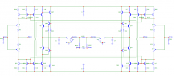
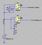
Hi Pavel, here is your circuit with some improvements.
Added degeneration resistors, changed the CM control injection method.
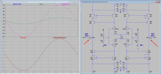
You can see the sim results in Screenshot 1.
Top pane shows the Differential path, bottom pane is common mode path. G stands for Gain.
Also cleaned the schematic a bit, but tried to make minimal changes.
Best, Sandro
P.S. Shameless plug 2: Don't forget to subscribe to my Youtube channel 🙂.
Added degeneration resistors, changed the CM control injection method.
You can see the sim results in Screenshot 1.
Top pane shows the Differential path, bottom pane is common mode path. G stands for Gain.
Also cleaned the schematic a bit, but tried to make minimal changes.
Best, Sandro
P.S. Shameless plug 2: Don't forget to subscribe to my Youtube channel 🙂.
Attachments

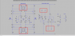
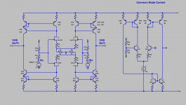
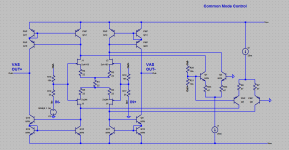
On the attached thumbs, it is difficult to locate the precise changed CM ctrl injection method nodes. I see abcd in the Diff GM section, but not in the CM ctrl section.
I was wrong because BesPav's initial circuit in #1 has exactly the same setup as my block diagram in #10 and not as I assumed a noninverting configuration. So the Zin on node IN- is R16: 2kΩ. Sandro cleared that up: thanks!
In my circuit (so actually the same basic topology now) I do not use current mirrors in the vas-sections and use low Zout followers, instead of straightaway the high Z vas output nodes. No CM control needed anymore as it appears!
Hi Mars, made the labels bigger just for you.
BesPav's circuit and my revision do not have a second stage (a VAS as many call it). It also does not have an output stage.
BesPav mentioned that he was planning on adding more stuff after the output's of the GM cell so I did not want to add anything and let him keep exploring the circuit.
MarsBravo: In my circuit (so actually the same basic topology now) I do not use current mirrors in the vas-sections and use low Zout followers, instead of straightaway the high Z vas output nodes. No CM control needed anymore as it appears!
If you post a schematic, I can comment, but I find it odd that you don't need a CM control.
- Sandro
Attachments
Last edited:
Thanks Sandro, obvious and expected, but now with spot on precision.
My circuit after the input stage deviates a bit from most fashional solutions; it is a 'vas' on steroids. Curious if BesPav's circuit needs CMctrl with low Z outputs. Can you simulate that with simple VCVS (voltage controlled voltage sources) as buffers?
But it is still a proof of concept only, the aim is to make a vas with an output impedance of sub 1Ω or even better 0.1 Ω without feedback. That's where my semi-triodes will kick in.
Can you simulate that with simple VCVS (voltage controlled voltage sources) as buffers?
Insert the VCVS as buffers where?
Made no difference... see image.
I used my buffer symbol. You can find info on it on video 4.2 🙂
Also, this circuit does not have a VAS. This is a single stage circuit.
[These are the days I feel like sending a letter to Douglas Self with a bomb inside for coining the forsaken VAS term]
I used my buffer symbol. You can find info on it on video 4.2 🙂
Also, this circuit does not have a VAS. This is a single stage circuit.
[These are the days I feel like sending a letter to Douglas Self with a bomb inside for coining the forsaken VAS term]
Attachments
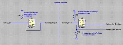
TIA, OTA and much more.Thanks! The AD844 acts as a symmetrical OTA in that way.
Also check attached, a way to lower input resistance of the current receiver itself (keep your fingers from making it negative) and improve linearity as Jan Didden suggests and Vadim Avkhimovich improve.
Hi Pavel, here is your circuit with some improvements.
Yeah, got it. Thank you for tidying!
Nice approach and since CM-gain of 1 are resistance tolerance tolerant. 😀
Now it's time to raise the loopgain and add some ThermalTraks.
Attachments
Made no difference... see image.
I used my buffer symbol. You can find info on it on video 4.2 🙂
Also, this circuit does not have a VAS. This is a single stage circuit.
[These are the days I feel like sending a letter to Douglas Self with a bomb inside for coining the forsaken VAS term]
Thanks Sandro and BesPav.
The buffer symbol is well known and in use 25+ years at least.
Somewhere else on diy this is well explained, and hence 'vas' not in capitals. Better transconductance and transimpedance stages.
The main differences between current BesPav's circuit and mine are the input diff not having a current mirror as load, and a referenced 'vas' preventing the floating high Z output. So the instrumentation approach is the same, but the build and stability is different. End of the hijacking now.
The resistor bridges R12--14 / R28--31 creating the injection nodes a b c d will degrade the open loop gain, as the signals from the input diffs runs through these now 'semidiffs' and add some signal of opposite phase into the opposite outputs of the input diffs. This is unavoidable because of the neccessary CMctrl injection in top and bottom current mirrors.
BesPav: Let's see what you come up with. Happy to help you on the journey.Now it's time to raise the loopgain and add some ThermalTraks.
Mars... I thought in Netherlands people were laid back... I was just joking with you. Of course I am aware you know what a buffer is.The buffer symbol is well known and in use 25+ years at least.
Better yet, "Second Stage". There has been enough fighting already on this "It is a TIS, not a VAS" nomenclature and I really do not want to go there. Also, in op-amp literature, "second stage" is widely accepted. Anyway, enough of that.Better transconductance and transimpedance stages.
The resistor bridges R12--14 / R28--31 creating the injection nodes a b c d will degrade the open loop gain, as the signals from the input diffs runs through these now 'semidiffs' and add some signal of opposite phase into the opposite outputs of the input diffs. This is unavoidable because of the neccessary CMctrl injection in top and bottom current mirrors.
If you look at the resistor values, the sum of the resistors is 2k (two 1k in series), which is 20x larger than the sum of the degeneration resistors, 100 ohms (two 50 ohm resistors). Therefore, the signal loss is small, ~5%. If you bump the 1k's to 5k's, then the loss will be 1% which is nothing.
Furthermore, if second stages are to be added then there will be plenty of open loop gain.
Shameless plug. We are, not always. Funny....in Netherlands people were laid back... I was just joking with you...
1 2 3 okAnyway, enough of that.
It is something to keep an eye on while raising the loopgain. My intuition points (fwiiw) a possible double loop with some gain and resulting overshoot or oscillation when phase margins become important. So R12--14 / R28--31 must stay high enough (relative) not to interfere with degredations R9-10 & R25-26 while maintaining the CMctrl injection to act sufficiently....the signal loss is small, ~5%. If you bump the 1k's to 5k's, then the loss will be 1% which is nothing...
That's BesPav's challange.
ComMode is surpressed also and no injection needed in the CurMirs at the expense of some offset in the input diffs. This should stay well within the Vgs+Vrs margins better...
Still, CMctrl is needed with this topo anyhow.
Still, CMctrl is needed with this topo anyhow.
It's better to understand how much loopgain/feedbackdepth are needed.It is something to keep an eye on while raising the loopgain.
Say, well optimised 3-stage emitter follower usually have something like -60 dB THD and for dropping overall THD to commonly accepted -100-120 dB you need not so much amplification inside the amp's core.
How about correcting the current at the source ?
Mona
Hi, Mona, thank you for your input!
That's an additional case to analyze.
At a first sight - not so much. Common mode loop in that case works in a current domain and common mode control loop have no Hi-Z load, so CM gain can't be huge.ComMode is surpressed
How about correcting the current at the source?
Also currents could be joined at the drains.
Attachments
- Home
- Amplifiers
- Solid State
- Bridged topology with common-mode control