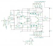
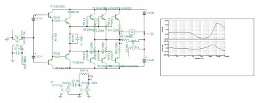
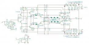
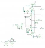
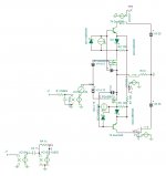
This is 250w voltage follower which requires to be explained.
First of all the Darlington is to be matched paired by applying a bc transistor who has inversly Hfe percentage to the output. That is, if the P output has 10% higher Hfe than the N , than the bc P transistor is to choose who's Hfe is 10% lower than the bc N. An ordinary multi meter with Hfe measuring can do the task.
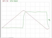
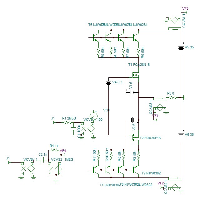
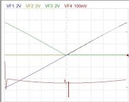
This output has two different types of feedback. The current sense resistors 0.1 ohm provide the drivers a feedback information to control the outputs. When the one driving the outputs sees the current it decreases its gain to adjust but the other one sees the idled output ,hence big error to releasing most of it's bias current . By this the active driver has most of its current pouring into the output. In this feedback the drivers do not see what is happening in crossover as it is the sum of both poles. The second feedback gets the sum of the two current poles by R31&32 and injects an inverse current to the input decreasing the gain by 10 fold . This feedback as ir sees the crossover cleans it thoroghly that even at 200ma total idle+vivid bias the crossover at 10khz 4A peak as shown bellow remains perfect. The distortion is 0.04% just to start with. The output current is inherently limited at -10A and +12A because the voltage drop of the sense resistors unbiases the active driver
Now That linearity problem is resolved , the frequency/pole character is to consider before refining further the distortion.
Attachments
Hi Hayk,
I ran you last TINA circuit. Thanks for posting the file. A bit hard to understand with this layout.
It works well at 10kHz. Nice work.
It seems to work much like the Blomley, eg run an LTspice sim here The Blomley Class B amplifier
Your circuit has added cascoded output transistors.
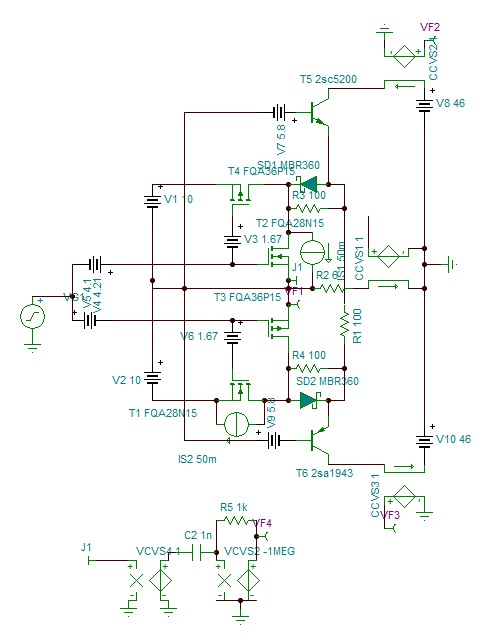
Your Schottky diodes (SD1,SD3) do the crossover, biased at 10uA and peaks at 160uA and this current is amplified by a fairly linear factor of 26,000 to give 4A peaks. And the output transistors are non-switching.
I ran you last TINA circuit. Thanks for posting the file. A bit hard to understand with this layout.
It works well at 10kHz. Nice work.
It seems to work much like the Blomley, eg run an LTspice sim here The Blomley Class B amplifier
Your circuit has added cascoded output transistors.
Your Schottky diodes (SD1,SD3) do the crossover, biased at 10uA and peaks at 160uA and this current is amplified by a fairly linear factor of 26,000 to give 4A peaks. And the output transistors are non-switching.
Last edited:
Hello Ian.
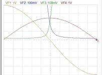
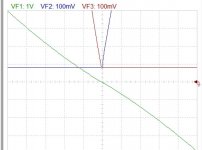
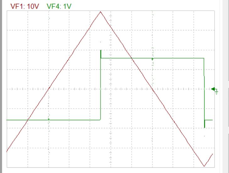
Today I took care about the frequency forgetting everything else. Indeed high idle bias does effect greatly . At this stage it shows it can accept just by a dominant pole at 20khz 50db NFB. That is the distortion of 20khz can be decreased by 300 fold. The sense resistors need a parasite 25nH inductance which can be done by wiring. It doesn't require any Lead capacitor across the feedback 10k , for now, but a pair of phase advance 22pf.
This is the dynamic transfer function at quiescent , Tomorrow , I see it with dc applied.
Hayk
Attachments
Class AB, 60-80mA per pair.
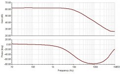
The measured performance is very close to the simulated.
I measured this configuration:
* 3EF open loop
* PSU +-50V
* predriver KSC3503,KSA1381, 1 pair
* driver 2SC4793,2SA1837, 1 pair
* output NJW0281G,NJW0302G, 3 pairs (rated power 200W/4R)
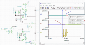
HELLO LKA.
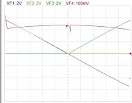
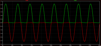
I tried out your circuit. Amazing, the output impedance although the input is current source measures 0.53 ohm up to 10khz to decrease above!! I didn't dig in what makes it so low impedance as I saw the linearity of it. The current generator is pounding the output with 4A 1khz triangle wave , not only the crossover is negligible but extraordinary linearity.The bias is 80ma/pair.
Attachments
Last edited:
So the people want linear class AB output? here is what has been promised.
10khz 5A peak current injected to the output.
The output is mounted in virtual amp. Although the distortion is 0.0003% at 1w/1khz it is 0.016% clipping 64.2v peak 257w. What intrigues me , the NFB factor I higher/lower it by 20db the distortion numbers remain unchanged , why?
10khz 5A peak current injected to the output.
The output is mounted in virtual amp. Although the distortion is 0.0003% at 1w/1khz it is 0.016% clipping 64.2v peak 257w. What intrigues me , the NFB factor I higher/lower it by 20db the distortion numbers remain unchanged , why?
Attachments
Last edited:
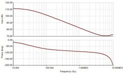
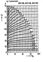
LKA, bad news. The spice model of bd transistors are wrong . I measured the model in complimentary 30ma , the picture bellow shows 1.250k ohm due to low early. In datasheet at so low currents the impedance is very high.
2SC4793/2SA1837 are my favorite drivers (still available from Unisonic), BD139/BD140 I used only in simulation, try SC/SA
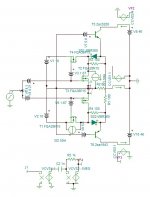
MOSFET classA square law
I switched to MOSFET outputs to get my desired transfer function of linearly varying transconductance. First I made it function in pure class A . I bestowed it with an armada of dissipating cascode transistors . The bias is 2A , but thanks to square law function instead of delivering 4A peak I get a bonus 2A extra to be 6A .
It can deliver 100w in classA 8 ohm with +/-46v rails.
Now, If I subtract the bias 2A current from the cascodes, I start getting my desired transfer.
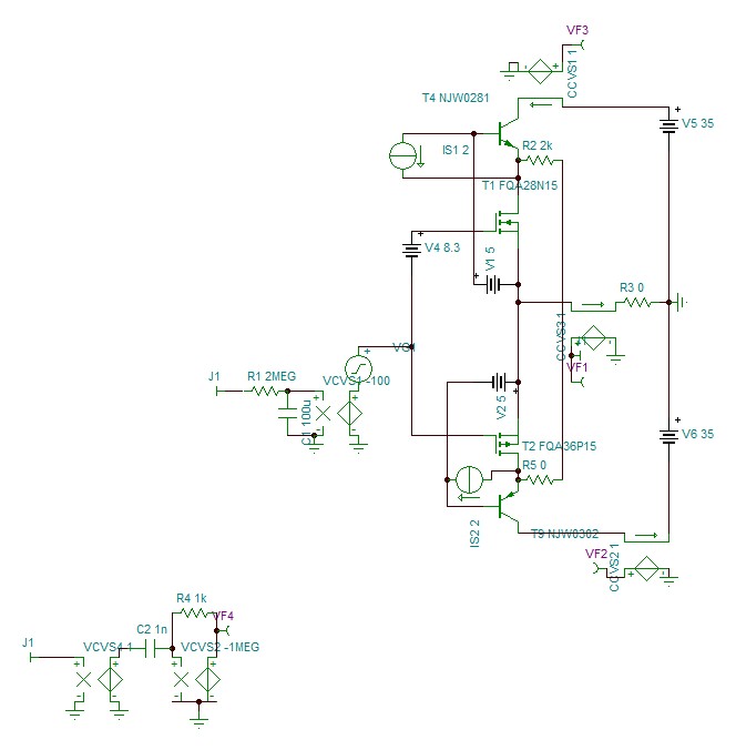
You can notice how I start getting a V shaped conductance curve.
Hayk
I switched to MOSFET outputs to get my desired transfer function of linearly varying transconductance. First I made it function in pure class A . I bestowed it with an armada of dissipating cascode transistors . The bias is 2A , but thanks to square law function instead of delivering 4A peak I get a bonus 2A extra to be 6A .
It can deliver 100w in classA 8 ohm with +/-46v rails.
Now, If I subtract the bias 2A current from the cascodes, I start getting my desired transfer.
You can notice how I start getting a V shaped conductance curve.
Hayk
Attachments

Hi Hayk,
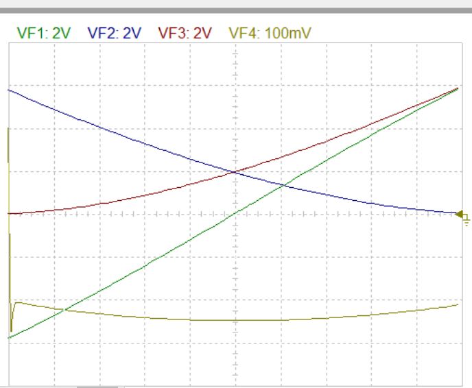
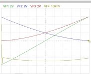
This methods causes the base-emitter voltages of cascode transistors (T4,T9) to reverse. See plot.
So it is not non-switching. It causes sharp gain wobbles at the crossover region.
Is there a way to make it non-switching? And remove the sharp gain spikes?
This methods causes the base-emitter voltages of cascode transistors (T4,T9) to reverse. See plot.
So it is not non-switching. It causes sharp gain wobbles at the crossover region.
Is there a way to make it non-switching? And remove the sharp gain spikes?
Attachments
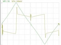
Good morning Ian. I made a quick sketch design early this morning to see if a classA can be converted into my desired function. Unfortunately the weather is cloudy here, so deprived from morning swimming . I did some preliminary modifications to see the feasibility , very promising.

The blue curve is not symmetrical as it should be, problem to resolve.
The blue curve is not symmetrical as it should be, problem to resolve.
Attachments
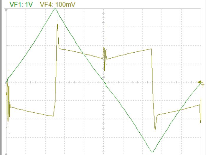
No, it doesn't go to zero. The cascodes have 80ma minimum to keep their Ft 40Mhz available instantly. For now I will shorten the inflation point to the lowest possible, that is the vortex of the V wedge is the sharpest , than I will give a roundness so that at inflation instead of going chaotic , it gets a constant slope.
No, it doesn't go to zero. ...
Hi Hayk,
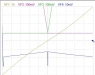
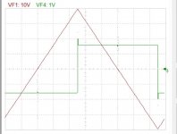
Here's what I said, "Now non-switching but you have a 0.5us zone where the output gain ramps down to zero."
Notice I said it is the "gain that ramps to zero". Where "gain" is the slope plot VF4.
I did see the non-switching rail currents of 81mA and 83mA.
The gap zone is adjustable. The problem to get perfect joint without over crossing. What troubles me is the complmentary missmatch that jumps suddenly from gm to the other. By better choice of Shottkys ultrafast UF5 from Diode, I get some enhancement .Paralleling the emitter diodes with resistors ,I get smoother overcrossing but disastrously too long constant slope at inflation point.
To match pair the MOSFETs , the P which has a lower gm needs to be biased at 2.15A when the N is biased 2A to have equal gm. the overcrossing is controled by two 100ohm resistors across the emitter diodes, for now. What is needed now is to halve the current of each at the crossover to keep the total gm constant.
Attachments
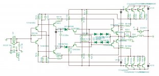
double push pull
This is another version of the precedent model where the dummy constant subtracting currents became active. This forms double push pull linearizing the outputs. The crossover provides sufficient margin , see the curves at 10khz. It can 133W @6 ohm all remaining classA.
This is another version of the precedent model where the dummy constant subtracting currents became active. This forms double push pull linearizing the outputs. The crossover provides sufficient margin , see the curves at 10khz. It can 133W @6 ohm all remaining classA.
Attachments
The gap zone is adjustable. The problem to get perfect joint without over crossing. What troubles me is the complmentary missmatch that jumps suddenly from gm to the other. By better choice of Shottkys ultrafast UF5 from Diode, I get some enhancement .Paralleling the emitter diodes with resistors ,I get smoother overcrossing but disastrously too long constant slope at inflation point.
One has to accept that complementary transistors are that in name only and they have some differences.
These which could be critical when it comes to turning them on and off - being mindful of stored charge effects and the time domain and transconductance curves.
If you elect not to turn these off you will have some lingering stored charges in the power transistor base regions. The question here is are these balanced to which the probable answer is no and if so what is there to do about that.
You could try using emitter resistors with slightly different values - to generate different value emitter feedback signals to compensate for some discrepancies in the complementary output pairs. Then you could try to close your gap.
The attachment is from a simulation for a simple low power Class AB circuit with a standing current of around 45 m.A. on 20kHz input 18V peak output into 8R. Slightly different emitter resistors improve the indicated THD result.
Attachments
It is hard to see an almost imperceptible step in the current near 0 A base line, about half way along ( see time base at 40uS and 160 uS approx) where the levels step up or down to align with the next step for that for the complementary device.
This strategy was used in an amplifier I built 30 years ago based on applications from an RCA Power Devices Manual for a 25W or 40W complementary symmetry amplifiers.
This strategy was used in an amplifier I built 30 years ago based on applications from an RCA Power Devices Manual for a 25W or 40W complementary symmetry amplifiers.
Looking good
Congrats Hayk!
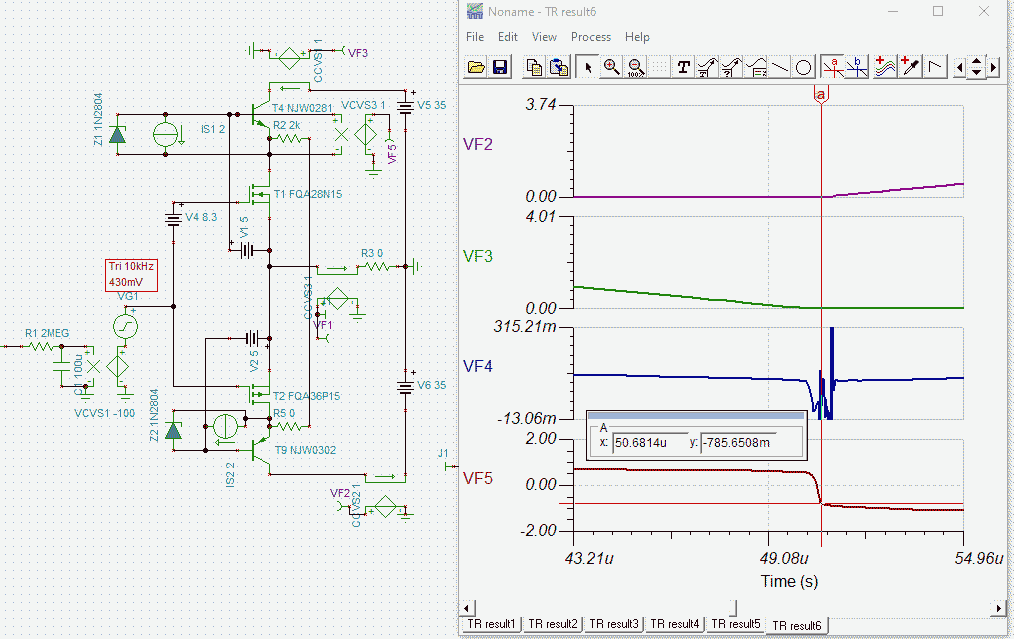
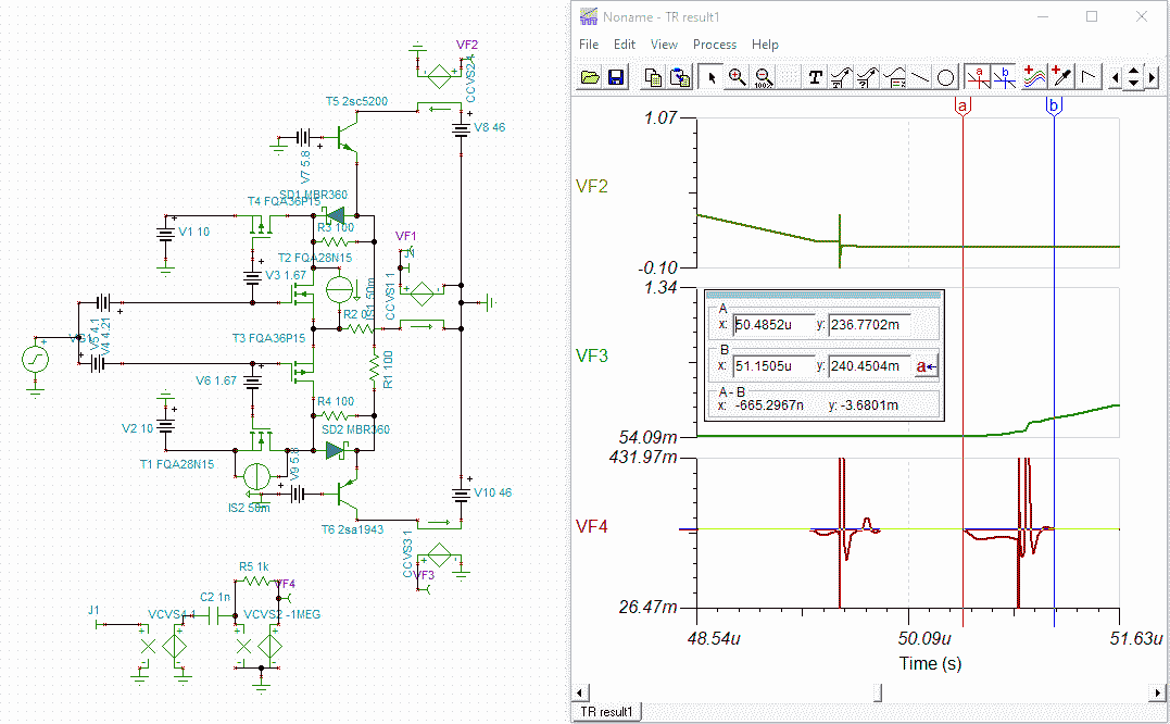
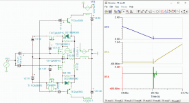
You have filled in the region where one output BJT is delayed in its turn on so a constant Gm . The plot below is the fist file you gave (without bootstrapped MOSFET supplies and BJT bases).
.
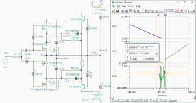
The second file with bootstrapped MOSFET supplies and BJT bases below:
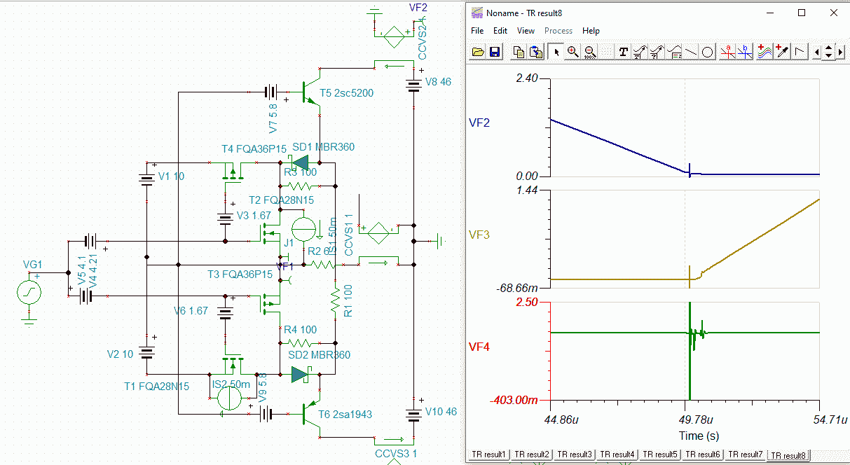
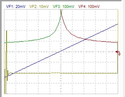
Both show the region before VF3 (current for T6) conducts at crossover and the gain is kept reasonably constant (apart from the gain wobbles which last less than 1us).
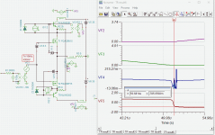
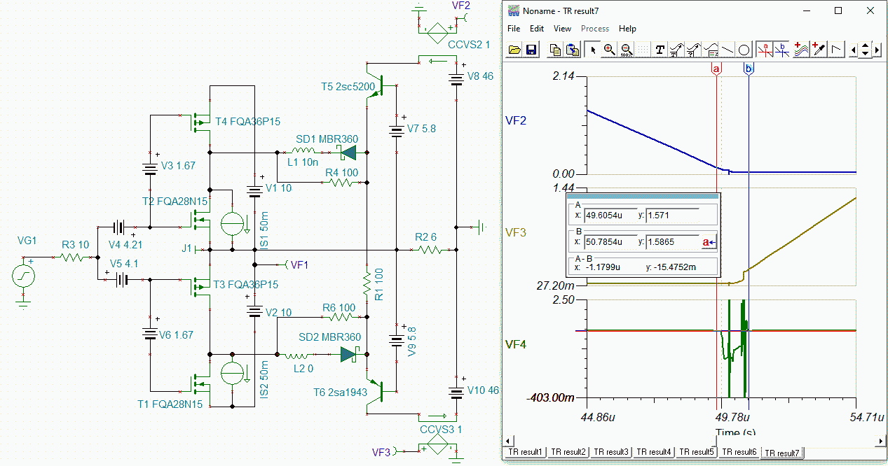
I was curious to see if a few cm of lead inductance in the Schottky diodes affected the circuit. Also the effect of 10 ohms gate drive source resistance which is a likely value for gate stoppers for HF stability. See the bootstrapped version below with some input resistance and lead inductance:
.
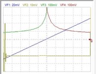
The gain wobbles now last longer (2us) and the Gm dips to about half in that region. This loss of gain will show up in THD simulations, but I don't know yet how much it will affect the HF end. The circuit I used is attached.
BTW the circuit looks a bit like the push-pull drive circuit I posted above (Posts 84, and mods 113,114,117). Yours differs in that your BJT's emitters are driven (common base) rather than the bases (common emitter). You use Schottky diodes in the emitters to make them non-switching. Nice idea.
BTW Common Base was used by Mills and Hawksford in their JAES Oct 1989 amplifier. It gives better linearity than the common emitter variant (because beta change with current and Early effect are significantly reduced with common base). But Common Base needs a high current driver with high linearity and this requires more power transistors, heatsink, and an extra power supply. Your MOSFET driver stage draws 2 amps with 20V rail-rail so dissipates 40W at idle -- compared to 10W for the BJT's. I tried reducing the driver supplies by half to 5V (to halve the idle dissipation) but this caused excessive nonlinearity; so the higher voltage (10V) seems to be needed for these driver MOSFETs.
Cheers,
This is another version of the precedent model where the dummy constant subtracting currents became active. This forms double push pull linearizing the outputs. ...
Congrats Hayk!
You have filled in the region where one output BJT is delayed in its turn on so a constant Gm
. The plot below is the fist file you gave (without bootstrapped MOSFET supplies and BJT bases)..
The second file with bootstrapped MOSFET supplies and BJT bases below:
Both show the region before VF3 (current for T6) conducts at crossover and the gain is kept reasonably constant (apart from the gain wobbles which last less than 1us).
I was curious to see if a few cm of lead inductance in the Schottky diodes affected the circuit. Also the effect of 10 ohms gate drive source resistance which is a likely value for gate stoppers for HF stability. See the bootstrapped version below with some input resistance and lead inductance:
.
The gain wobbles now last longer (2us) and the Gm dips to about half in that region. This loss of gain will show up in THD simulations, but I don't know yet how much it will affect the HF end. The circuit I used is attached.
BTW the circuit looks a bit like the push-pull drive circuit I posted above (Posts 84, and mods 113,114,117). Yours differs in that your BJT's emitters are driven (common base) rather than the bases (common emitter). You use Schottky diodes in the emitters to make them non-switching. Nice idea.
BTW Common Base was used by Mills and Hawksford in their JAES Oct 1989 amplifier. It gives better linearity than the common emitter variant (because beta change with current and Early effect are significantly reduced with common base). But Common Base needs a high current driver with high linearity and this requires more power transistors, heatsink, and an extra power supply. Your MOSFET driver stage draws 2 amps with 20V rail-rail so dissipates 40W at idle
-- compared to 10W for the BJT's. I tried reducing the driver supplies by half to 5V (to halve the idle dissipation) but this caused excessive nonlinearity; so the higher voltage (10V) seems to be needed for these driver MOSFETs.Cheers,
Attachments
- Status
- This old topic is closed. If you want to reopen this topic, contact a moderator using the "Report Post" button.
- Home
- Amplifiers
- Solid State
- Non-switching complimentary output stage