Good morning Ian.
The original theme of the thread is "Non-switching complimentary output stage" , in general, not a certain amplifier.
Hayk.
The original theme of the thread is "Non-switching complimentary output stage" , in general, not a certain amplifier.
Hayk.
Hi Hayk,
That's helpful to know.
But I still don't know if you want me to post more on this theme here.
That's helpful to know.
But I still don't know if you want me to post more on this theme here.
Last edited:
Everyone , particularly you , are welcome to bring ideas . After all ,this is an open source project.
An only just non-switching amp?
Hi Hayk,
Thanks for the reassurance. I didn't want to be a thread hijacker🙂.
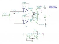
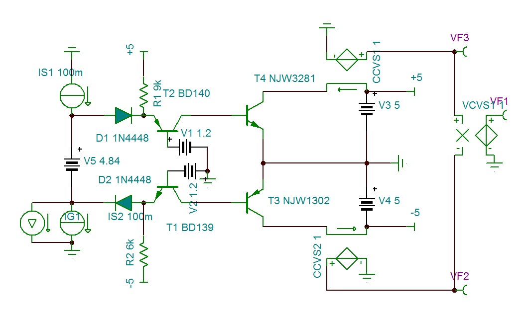
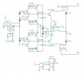
My variation uses push-pull drivers enabling good pull-out of base charge at high frequencies.
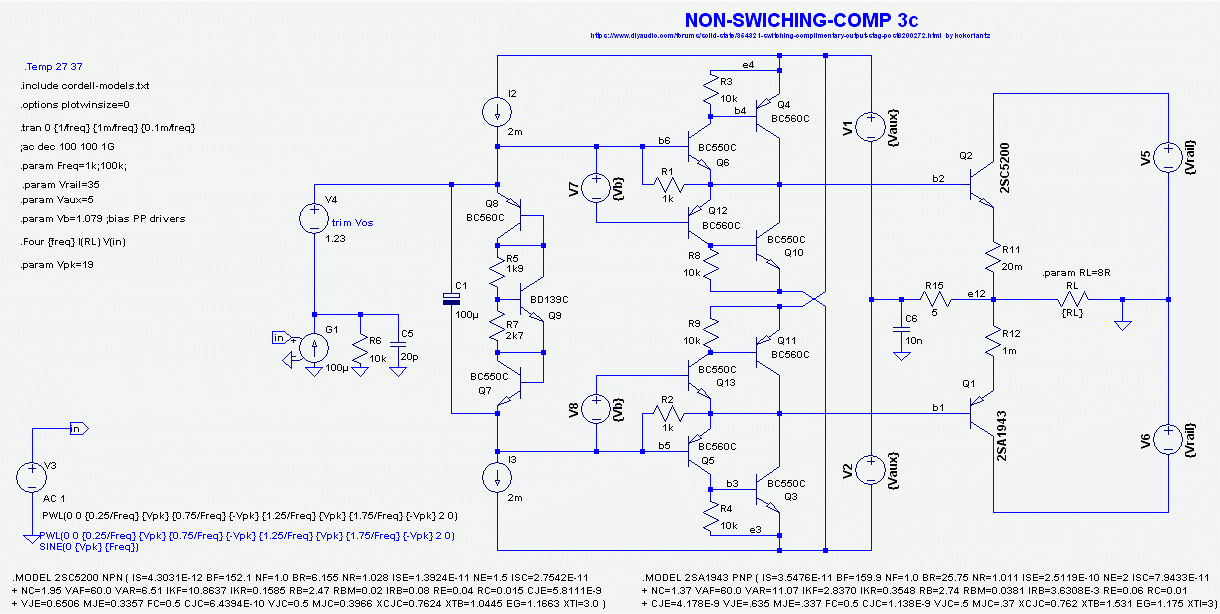
V7 and V8 bias the PP drivers for around 1mA through Q4,Q10 (and Q11,Q3 same 1mA). The same 0.5mA flows through R1 and R2 for non-switching except now it gets progressively lost to Q10 and Q3 at higher input voltages.
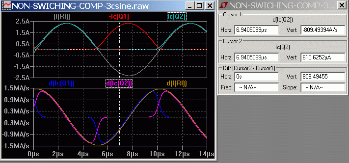
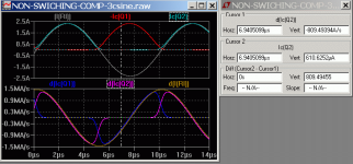
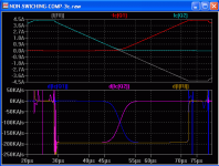
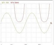
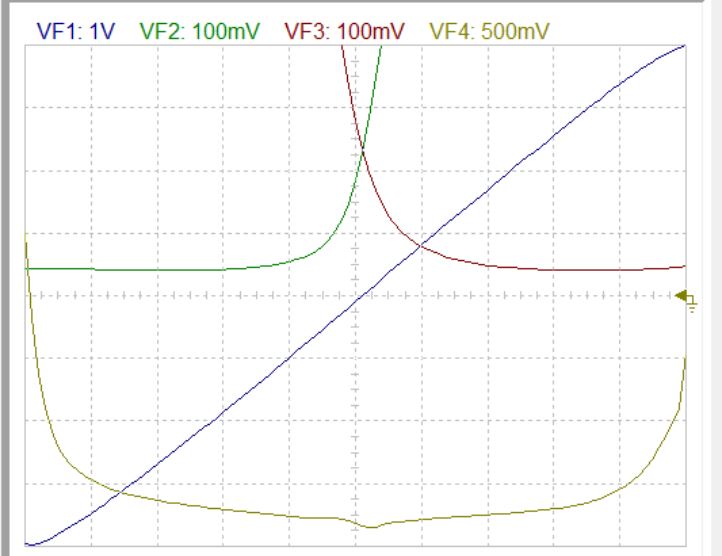
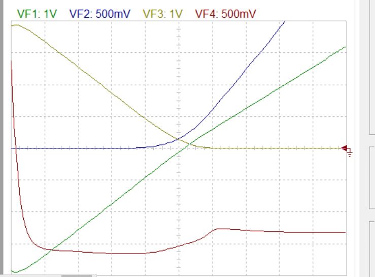
Still, a small current flows in the 'off' power transistor (and some gm!) even at high input voltages, seen below with 100kHz with 165mA bias in output tr's
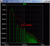
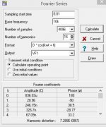
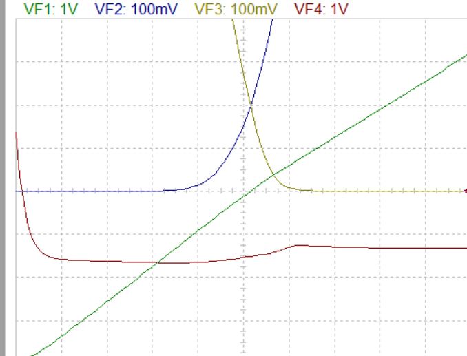
The sacrifice of most of the non-switching current is good control at 100kHz; THD with 19Vpk is 0.06% at 100kHz. It's 0.038% at 1kHz or 0.04% at 20kHz (all same 165mA bias). FFT at 20kHz below

Harmonics fall away quickly for (potentially) a good sounding amplifier. At 1W 20kHz THD is 0.0023%.
R15 and C6 are effectively a Zobel network that damps ringing with a triangle wave or recovery from a rail clip (something I learned from you🙂). C5 provides most of the compensation with R6.
One advantage over the standard 3EF is the bootstrapped drivers have low voltages with small dissipation allowing small-signal transistors with high FT's. Alternatively, the stage can have some voltage gain using floating main power supplies (then the driver supplies are ground referenced).
This is just the proof of concept. V7,V8 could be incorporated into the other bias generator somehow, probably with independent adjustment of the PP idle current to the output pair bias. This is opensource so anyone can suggest ways to do it.
It looks promising - although (as implemented here) it is borderline in terms of being truly non-switching. Maybe it should be called an "only just non-switching amp"?🙄
Hi Hayk,
Thanks for the reassurance. I didn't want to be a thread hijacker🙂.
My variation uses push-pull drivers enabling good pull-out of base charge at high frequencies.
V7 and V8 bias the PP drivers for around 1mA through Q4,Q10 (and Q11,Q3 same 1mA). The same 0.5mA flows through R1 and R2 for non-switching except now it gets progressively lost to Q10 and Q3 at higher input voltages.
Still, a small current flows in the 'off' power transistor (and some gm!) even at high input voltages, seen below with 100kHz with 165mA bias in output tr's
The sacrifice of most of the non-switching current is good control at 100kHz; THD with 19Vpk is 0.06% at 100kHz. It's 0.038% at 1kHz or 0.04% at 20kHz (all same 165mA bias). FFT at 20kHz below
Harmonics fall away quickly for (potentially) a good sounding amplifier. At 1W 20kHz THD is 0.0023%.
R15 and C6 are effectively a Zobel network that damps ringing with a triangle wave or recovery from a rail clip (something I learned from you🙂). C5 provides most of the compensation with R6.
One advantage over the standard 3EF is the bootstrapped drivers have low voltages with small dissipation allowing small-signal transistors with high FT's. Alternatively, the stage can have some voltage gain using floating main power supplies (then the driver supplies are ground referenced).
This is just the proof of concept. V7,V8 could be incorporated into the other bias generator somehow, probably with independent adjustment of the PP idle current to the output pair bias. This is opensource so anyone can suggest ways to do it.
It looks promising - although (as implemented here) it is borderline in terms of being truly non-switching. Maybe it should be called an "only just non-switching amp"?🙄
Attachments
Last edited:
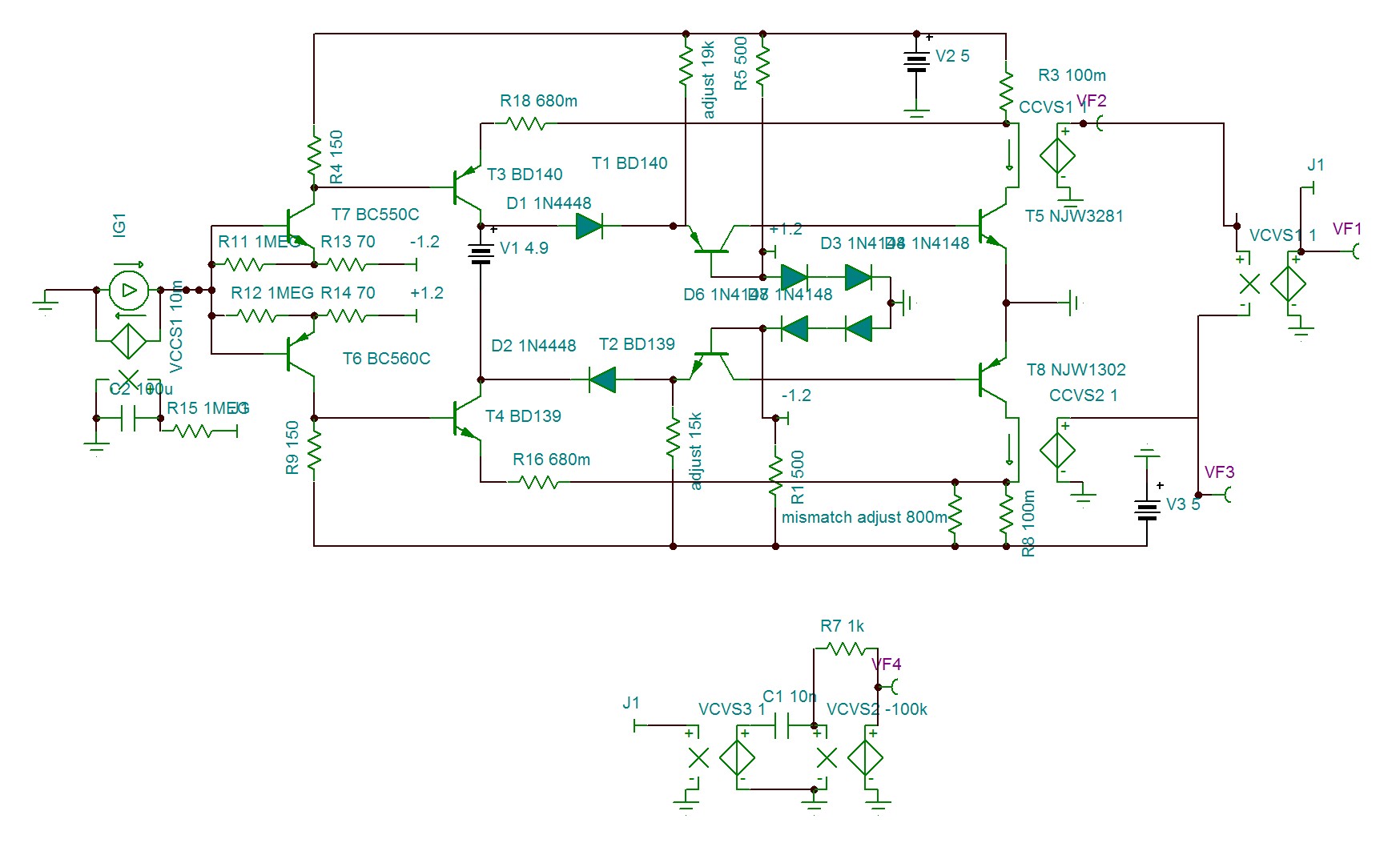
I also reached the same conclusion as you , push pull for each. Only my way doesn't have voltage biasing but simple pull up as you had in your original circuit . In fact mine is the next step of the old circuit I show on post 39. If you understand how it is biased you will be amazed. It's crossover is perfection but switches off. Say that such a jewel people discard it even by Jan Didden because old technology. I call this circuit Helen , after a song of George Brassans , Les sabots d'Helen.YouTube
Last edited:
Ian, you will not show the transfer function? . You need to obtain on the output triangle wave of 5A peak by an input of current generator . Add a derivative of the output current .
Which impedance? Which Re?...where the impedance is half the Re of the transistors...
How do you measure that?...The knee for C5200&Co is situated at 900ma, measured in real world , where as TTA&Co was 500ma...
I have both Toshiba datasheets (2S<>TT) ready for reference if needed.
On Ic/Vbe curve get the maximum slope , divide it by two , bring the half slope to touch the curve you get the knee. Re is the internal emitter resistance describe by the maximum slope . If I remember C5200is 0.012-0.015 ohm. To link the two emitters you can understand that just 1cm of lead is disastrous , for that , I cutt the emitter leads until the flat part, and mounted the two transistors on the heat sink opposite to each other so that the two emitter short flat pins come one on the other and solder.

On Ic/Vbe curve get the maximum slope, divide it by two, bring the half slope to touch the curve you get the knee. Re is the internal emitter resistance describe by the maximum slope.
Can you give an estimation where the max slope in the curves is and at which temperature and why that temp?
Devide the slope by two...?
...bring the half slope to touch the curve...?
I'm not sure how to point a maximum slope on a exponential curve, even if this curve is not exponential all the way. Math say infinite, but the reciprocal yields zero ohm.
Attachments
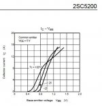
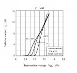
It seems to me the curve of the 2SC5200 is (more or less) straight from 2 to 10A @ 25º (2 to 8 @ 100º), ditto TTC5200 from 1 to 5 @ 25 (wobbly at 100º), so admitted there is a difference (although both Toshiba made). But how do you determine those very specific values of 4 and 2 resp from these course curves?
Next divide 4A by 2 (= 2A), and 'bring the half slope to touch the curve'...
That's (@ 2A) where it becomes visable that the curve is actually exponential, but again, in this course graph specifically. Do you have access to more detailed graphs?
Next divide 4A by 2 (= 2A), and 'bring the half slope to touch the curve'...
That's (@ 2A) where it becomes visable that the curve is actually exponential, but again, in this course graph specifically. Do you have access to more detailed graphs?
Here?Ian, you will not show the transfer function? . You need to obtain on the output triangle wave of 5A peak by an input of current generator . Add a derivative of the output current .
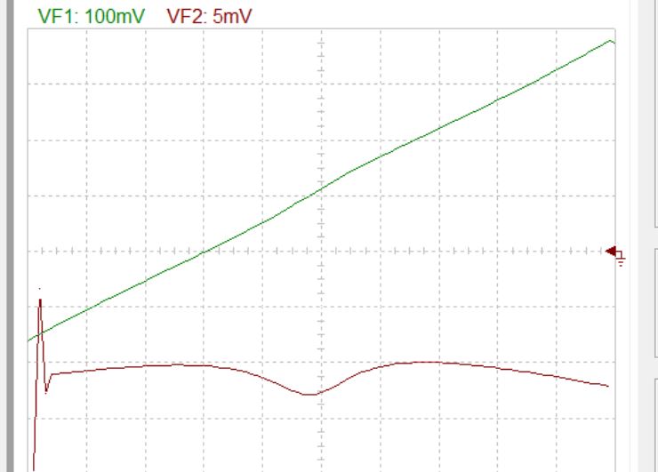
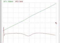
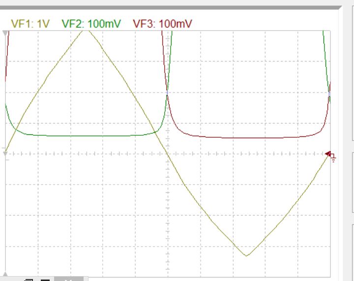
Lower plots are derivatives (upside down).
The derivative of the output triangle is required at 10khz to show absence of discontinuity as classA can do. These curves are impressive all being doubtful what ? makes is so linear.
Your output current is only 2.5A p , make it 5A
Your output current is only 2.5A p , make it 5A
Last edited:
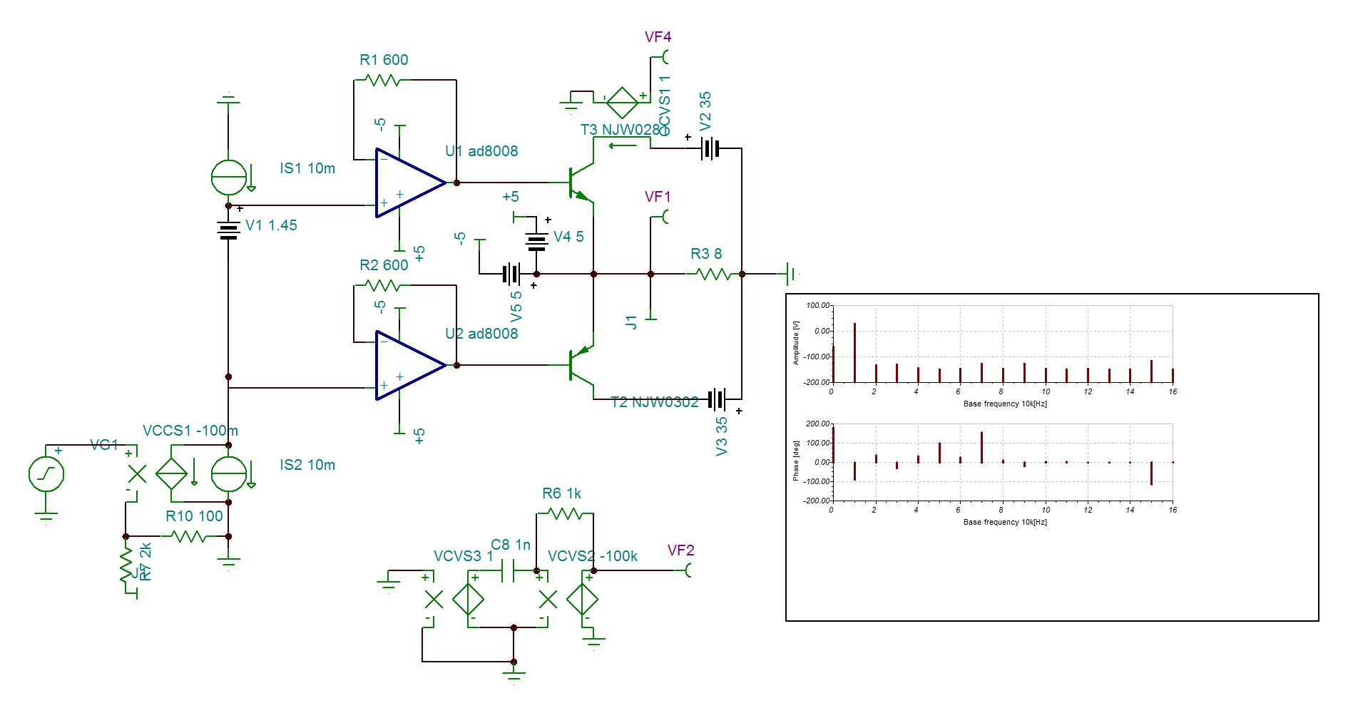
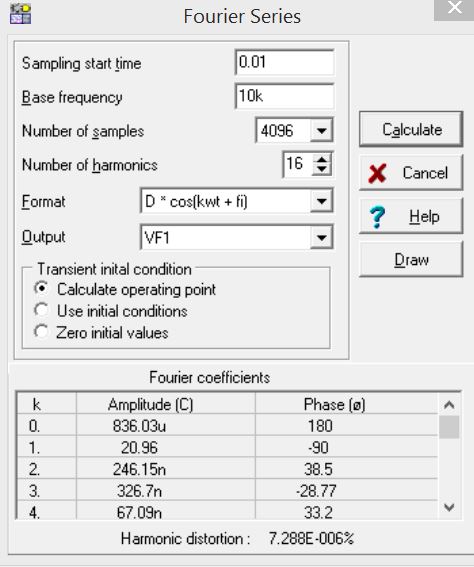
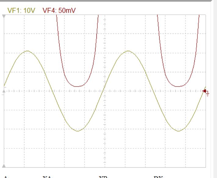
I made a quick model using AD8008 CFA op amp 450Mhz unity gain instead of your buffers. Indeed by using NJW0281 indicated to us by LKA , the result is very near to perfection. While with the Japanese ones ,??? good but not so good. Thank you LKA once again .
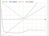
Note: The V2 scale is 5mv VS 10mv for the C5200
Note: The V2 scale is 5mv VS 10mv for the C5200
Attachments

Last edited:
Making a virtual amplifier with the above circuit with 0.1S gain, The distortion at 20vp 10khz is simply the noise. The amp is a non-switching as it works in square low with only 250ma,. The low early character is also helping to keep the current flow at high Vce voltage . For once the early makes good. With the precedent configuration test with early effect inhibited , when one was pouring 5A , the other had still about 100ua to deal with.
Attachments
Give Caesar, what is to Caesar, to Diode , what is to Diode
Since the beginning , the complimentary output stages use the transistors as diodes in crossover region , relying on their Ic/Vbe character , and as BJT transistors with beta Hfe function in outside crossover region. To get perfect crossover , the diode characters of P & N should be exactly identical, regardless the frequency , which is never the case. Adding the temperature drift and all the trallalla that goes with, it is wrong way to use the transistors. I , who always followed roads that don't lead to Rome , decided to dedicate a pair of identical fast switching diode to perform the crossover function and leave the transistors to perform their natural current multiplying function.
The deformed negative part of the curve is due to Hfe mismatch that the spice model purposley has 20% .The driver and predriver now must now required to adjust the mismatching .
Vincero , VINCeeeRO.
Attachments

Last edited:
EUREKA EUREKA EUREKA
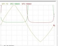
By feedbacking the output current to the driver, The mismatch is adjusted by the sense resistor . The most strange , the resonance at the peak slope reversal of the triangle wave , instead of being worsened by the feedback , on the contrary it totally vanished. Now the output is far superior to the best class A amplifier.
Now , 60 years of class AB research ,has achieved.
10khz 4A bias 230ma.
Next , to adapt the cascode , while reducing the quiescent passing through .
Attachments

Hello Ian.
I tried out your circuit . The crossover joint is excellent , but the deference of Hfe of the outputs is exhibited.
What makes your circuit unusable is it's very low beta, Iout/Iin =200 only. That is the 8 ohms is reflected as 1600 ohm , or I made a mistake in copying.
What the 5 ohm in series with the foating supplies does serve for?
It looks to be switching.
Attachments
Last edited:
- Home
- Amplifiers
- Solid State
- Non-switching complimentary output stage