


This is a realisation of Papa Nelson F5 by Fab of Fabaudio FSSA class AB amplifier.
I made this amplifier with full carbon resistors. I wanted a high end Lateral mosfet to drive very difficult 4 ohm {2.4ish actual) with my own twist. A more musical yet powerful amplifier. It will be driving nht speakers and kharma GLE. Both very power hungry.
It's powered by Swedish lindersberg transformer. 26vac. Output to a speaker protection. Diy slowstart using h3y omron. 4x10000> Inductor >5x10000uf capacitor. I already tried capacitance multiplier but decided this is a better approach to achieve a more textured rich sound.
I'm using Ecw series. Dual transistor per die. 35vdc ct 400ma and above. Was told by Papa Godzilla that I could get 100w. With about 4 percent class a.. Whatever that means.
I'm progressing very slowly for this one as I want it to look great and sounds great. I had thus pcb for 6 months and slowly collecting parts. Learning while building. So I only post it now as it's near completion. I am not well verse with any electronic's theory. But a buddy of mine who reviewed the circuit said.. This iwill be worth the effort. Do it. Thus a more serious effort.
Fab makes absolutely great build manual. It's very easy to build. And he is also great in supporting this build. I have some difficult to get parts and got help. And also a couple of transistors replacement. Ztx795 is not easy to get here so I replaced with bc639 and bc 640. Eveyrhing is matched as closely as I could. Since I'm a noob doesn't hurt to be more careful.
Last edited:


Hi AnthonyA
Thanks for sharing your build.
With 400ma of bias you should get about 2W in class A into 4 ohms considering the square law effect of mosfet. But it is a class AB design. If your speaker are efficient than at normal listening levels you should be mostly in class A. With your heatsink you may consider going higher bias than 400ma.....and your cats may like the warmth it will create...😉
For output transistors location on heatsink the optimal position is lower than half the height of the heatsink because heat flow goes toward the top.
What type of insulator you have for output transistors?
Fab
Last edited:
That's great Fab,
I'm using mica now as insulator but I have ceramic on the way. I also stretched it as far as I could .the pcb is on bottom half so , the transistor less than 1/2 way down.
Also I had drilled the transistor 4mm .so I could use m4. Yes I'd possible I prefer 800ma or so .since only 36vdc ct
Question 1,
Anyway I think r40 and r41 I followed the fssa1 as 10k
So test part 2 .p3 I can only turn to minimum1.4 v instead of 0.8v is that ok to go ahead? Presumably 800ma
Question 2
M3 on pcb ecw20n20
M4 on pcb ecw 20p20
Correct?
Let's keep discussion here ..email gets too complicated to see
Last edited:
Hi AnthonyA
Excellent for position on heatsink then.
R40/41 as 10k is ok since it simply reduces the max open loop gain further more then 22K ohms. Thus reduces feedback factor. Try it and you can always try 22k later maybe...
Yes you are right for test 2 that 1,4 vdc will work as well but will be closer to final bias and since you intend to go higher than 400ma that should be fine. I will eventually recommend P3 as 1K instead of 500 ohms to allow more room for bias adjustment.
Yes M3 is N channel and M4 is P channel.
Fab
Last edited:
Based on your vbe multiplier range I estimate your Q5 vbe about 0.8vdc which is higher than expected. That explains the higher vbe multiplier value. I estimate your final bias will vary between 200ma to maybe 800-900ma with P3 but that depends on your specific mosfet installed. The vbe multiplier range was not meant to give such high value. I suggest that you try it like that to obtain your target bias or close to. 800ma is a lot for class AB so 700ma would be fine too.😉
In the next manual iteration I could provide more option for the vbe multiplier for opération at higher bias.
Fab
In the next manual iteration I could provide more option for the vbe multiplier for opération at higher bias.
Fab
Last edited:
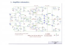
Schematics of FSSA2
This may not be the exact latest version for parts values but it gives the idea.
D7/D8 voltage should be roughly about half the power supply voltage value.
Fab
This may not be the exact latest version for parts values but it gives the idea.
D7/D8 voltage should be roughly about half the power supply voltage value.
Fab
Attachments
Last edited:
Still not wanting to be stable. Had to burn in some
80ma on driver
600ma on final
Wait a bit
The offset and bias is still drifting alot
80ma on driver
600ma on final
Wait a bit
The offset and bias is still drifting alot
Last edited:
That is why the ZTX transistor is suggested in section 8 for Q5 since it supports up to 500ma compared to 100ma of the BC type. So the ZTX is more forgiving during driver current adjustment. But BC type is ok for 50ma. Re-adjust P1/P2 until 50ma max driver current. This process is iterative and can take several minutes after power-up . Ensure your thermistors are working. If you lift a bit one thermistor you should see a noticeable change in driver current and dc offset.
Output bias should be stable because of the vbe multiplier and mosfet temperature coefficient after about 20-30 minutes.
Dc offset needs to be re-adjusted after at least 30 minutes after power up. It is only then that you can target 5mv or so. 10mv or 20mv is fine too without any detrimental effect on sound.
Fab
Last edited:
475 yes.
I got Ntc locally luckily I bought a better one as well
600ma slightly warm
50ma driver.
All good.. It's raining cats and dog and big thunderstorms... Shut down all expensive equipment.. Later
I got Ntc locally luckily I bought a better one as well
600ma slightly warm
50ma driver.
All good.. It's raining cats and dog and big thunderstorms... Shut down all expensive equipment.. Later
A different part number of ntc even with same nominal value at 25C will have a different resistance -temperature curve.
Fab
Fab
I got problem buying from those digikey mouser.. Anyhow if still have issue I'll need your help to order. Didn't know it's different.
If I knew I would have sent you the ntc which I can get easily from the distributor. In the mean time you can bypass R11/12 to start with. If it over compensate then you can use an intermediate value between 0 and 475 ohms.
Fab
Fab
Last edited:
- Home
- Amplifiers
- Solid State
- FSSA amplifier build thread with review