Have a look at this, but have a read at all the thread.
3 stage LIN topology - NFB tappings?
Also download this pdf called 'How to Wire up an Amplifier':
Ground Loops
3 stage LIN topology - NFB tappings?
Also download this pdf called 'How to Wire up an Amplifier':
Ground Loops
Attachments

If that is cause of all this trouble, I will remove D5 and D6, the parallel capacitors, and replace them with 22 Ohm resistors. Without those diodes the bias voltage requirement will be lower and I will have far more control over it. The reason is for the same preset change, the change in bias voltage will be lower as the multiplying fact of the VBE multiplier would be lower. As it is, the factor is about 4, without the diodes, it will be about 2.
The diodes drop about 0.6V which is in series between your voltage multiplier and the driver bases so the voltages present at those points should increase in each case.
Looking further afield you have three diodes D10-D12 feeding the base of your Vas transistor Q4 which is probably tied down to around 12V due to the path to Q20 and the 12 volt biasing from D3.
Get rid of D10-D12 - if you need protection for Q4 you can use a PNP transistor to sense the emitter resistor voltage drop (R7) to steal some base current.
As the result of the foregoing Q4 collector voltage should increase and you should set your Vbe adjustment for minimum current and take set up safety precautions.
You need higher voltage rated transistors like 2N5551 and 2N5401 to replace the BC types in your input stage.
The driver bases parallel capacitor and diode arrangements have been replaced with a 22 Ohm resistor.
I tried the amplifier with the new changes and successfully set a bias voltage. Touching the plastic case of the VBE transistor with a finger was enough to sense my finger's temperature with the corresponding drop in the VBE bias voltage. This transistor is meant to adjust the bias with changing temperature. The fact that it responded to heat by reducing the bias, is an indication that the amplifier will handle higher temperatures as it should, but I need more tests to confirm that.
I tried the amplifier with a Classical Music piece and was satisified with its performance. I also tried other music pieces, and it seems it will make a decent amplifier, but all this will cost me a lot of patience, as with any hobby.
I changed two VBE multiplier resistors to get a lower voltage setting that is about 1.2V. The VBE bias should now be correct.The diodes drop about 0.6V which is in series between your voltage multiplier and the driver bases so the voltages present at those points should increase in each case.
Since this circuit is already built, I don't have much freedom of redesign. Therefore, I am trying to keep my changes to a minimum. LTSpice simulations never showed this is a problem. The distortion figure is also very good, about 0.03% @ 1KHz and 0.9% @ 16KHz.Looking further afield you have three diodes D10-D12 feeding the base of your Vas transistor Q4 which is probably tied down to around 12V due to the path to Q20 and the 12 volt biasing from D3. Get rid of D10-D12 - if you need protection for Q4 you can use a PNP transistor to sense the emitter resistor voltage drop (R7) to steal some base current.
I purposefully used a high voltage cascode to enable the use of low voltage input transistors. The current mirror does not need high voltage transistors as the voltages there are always below 5V. 5V being an over estimate. The differential pair transistors are only exposed to the voltage at the cascode's emitters. This voltage is set with the use of a Zener diode at about 8V or so.You need higher voltage rated transistors like 2N5551 and 2N5401 to replace the BC types in your input stage.
I tried the amplifier with the new changes and successfully set a bias voltage. Touching the plastic case of the VBE transistor with a finger was enough to sense my finger's temperature with the corresponding drop in the VBE bias voltage. This transistor is meant to adjust the bias with changing temperature. The fact that it responded to heat by reducing the bias, is an indication that the amplifier will handle higher temperatures as it should, but I need more tests to confirm that.
I tried the amplifier with a Classical Music piece and was satisified with its performance. I also tried other music pieces, and it seems it will make a decent amplifier, but all this will cost me a lot of patience, as with any hobby.
Attachments
Understanding earth loops:
First of all, thanks to Mooly for posting those links. I would like to read a scholarly paper that explains the theory behind earth loops. By earth loops I am also including ground loops.
So far, my understanding goes as follows as described in the following text.
The problem with earth loops is the fact that the signal is supplied by the source and is used to drive the input of another independent circuit. This means, if the voltage drops across the signal ground and the amplifier gound do not cancel each other, a current will flow in the ground loop so formed. Since this current has nothing to do with the signal and uses the ground through which the signal is applied, this will superpose on the signal causing ground interference.
In my amplifier circuit making the ground contact at the 0V track near the large smoothing capacitors is what logically makes sense. These tracks are large tracks from the original circuit board, therefore their design should be optimal.
The ground terminal will be connected to the large heatsinks that will be in direct contact with the amplifier metal box. The box is already earthed. The wiring is still intact from the factory.
Mooly, tomorrow I will give the amplifier a day long test. I also tested the VBE multiplier's response to temperature increase and noted the VBE bias dropped with increasing temperature. This is very promising for me.
I downloaded the following scholarly document about earth and ground loops. I want to understand precisely what goes on.
http://web.mit.edu/jhawk/tmp/p/EST016_Ground_Loops_handout.pdf
http://web.mit.edu/jhawk/tmp/p/EST016_Ground_Loops_handout.pdf
I found that it helped my understanding of the issues to simply think in terms of a DC amplifier.
Draw it as an opamp with wires from the various important nodes and power supplies and then assign crazy resistance values to those wires. Say 1 ohm.
Now look at what the opamp output would do if you had say 1 amp flowing in that wire. This 1 amp could be ripple current between capacitors... but keep it DC just to think about the problem.
Lets say you looked at your 1 ohm ground lead. If the length of wire had the input ground and the feedback return connected to it at various points along its length then you would of course see a voltage difference along that wire. Those differences in voltage between the nodes would be amplified by the opamp… result is unwanted output.
The aim is to have the amplifier work correctly even with large value resistances for all the conductors. Make the wiring 'disappear' electrically.
The temptation is becoming stronger!
I am testing the amplifier for extended periods of time by playing music. The fact that the amplifier is stable is tempting me to test it using half the target voltage of +/-85V DC. I can achieve this by using a large autotransformer that has a single centre tapped coil. The transformer is a veteran WWII transformer rated at 1500W and is quite heavy.
I understand with these ratings even half the voltage is catastrophic in the event of an incontrollable current.
 only you can answer that one... hopefully all will go well.
Some possible attention to detail
With four power devices per output half it is going to be that much more difficult to match current gain and current sharing of devices in each half. I doubt 0.22 Ohm emitter resistors are going to promote that to the degree required.
While you are operating at half voltage supplies this is something you can do as an intermediate check by measuring the voltage drops across each output transistor emitter resistor and deducing the current from Ohms law.
You could moderate any disparaties by fitting low value stopper resistors in the bases - I used 2.2 Ohms in an earlier simulation it was a minimalist perhaps, the value might be double this on real hardware.
For another thing I recommend reverse connected rectifier diodes between the output line and the supply rails. When the protection circuit activates there needs to be a discharge route in either direction for the energy generated by the loudspeaker in motion.
Without this provision there is risk of blocked energy build up taking out power transistors.
I note the feedback path is made from two series resistors which raises the question where are these placed physically. I believe would be better to replace the one furthest away from the inverting input terminal and replace the closest one to that point with 12k.
I am testing the amplifier for extended periods of time by playing music. The fact that the amplifier is stable is tempting me to test it using half the target voltage of +/-85V DC. I can achieve this by using a large autotransformer that has a single centre tapped coil. The transformer is a veteran WWII transformer rated at 1500W and is quite heavy.
I understand with these ratings even half the voltage is catastrophic in the event of an incontrollable current.
With four power devices per output half it is going to be that much more difficult to match current gain and current sharing of devices in each half. I doubt 0.22 Ohm emitter resistors are going to promote that to the degree required.
While you are operating at half voltage supplies this is something you can do as an intermediate check by measuring the voltage drops across each output transistor emitter resistor and deducing the current from Ohms law.
You could moderate any disparaties by fitting low value stopper resistors in the bases - I used 2.2 Ohms in an earlier simulation it was a minimalist perhaps, the value might be double this on real hardware.
For another thing I recommend reverse connected rectifier diodes between the output line and the supply rails. When the protection circuit activates there needs to be a discharge route in either direction for the energy generated by the loudspeaker in motion.
Without this provision there is risk of blocked energy build up taking out power transistors.
I note the feedback path is made from two series resistors which raises the question where are these placed physically. I believe would be better to replace the one furthest away from the inverting input terminal and replace the closest one to that point with 12k.
A few more ideas
I expect by now having read the material associated with correct earthing - including the radiated effects of output stage switching.
The closed loop gain of your circuit is high at 68 times and consequently with the lowish value of the decoupling resistor 180 Ohms to earth in combination with a capacitor has to be high - you have 2200uF which physically would be relatively large. With radiated emissions and this being sited next to an amplifier input you don't want this to serve as an aerial to those sources.
With parallel diode protection of this component halving the closed loop gain parallel diode protection a lower capacitance value and a lower working voltage choice would result in a physically smaller fit.
Of course the 180 Ohm resistor would need to be doubled to halve closed loop gain and to retain the roll off point you would need only 1000uF but you could go as low as 220uF - 330uF without noticing much difference.
You could balance the shortfall in power amplifier gain by using a control amplifier ahead of this - possible with a IC prototype board and a dual op.amp with a closed loop gain of two and site the circuitry remotely.
In the power amplifier it is not a bad thing to arrange for the feedback resistor to be placed in a plane at a right angle to the orientation of output stage emitter resistors. If you don't have things this way this advice might have come too late to change.
So, to get a clean input interfacing one needs to cancel out all interfering signals that use the signal ground as their passage. Reading has again confirmed that the best input interface is one which has the ability to cancel out all interference signals, and this, without doubt, is the honourable balanced input. However, this amplifier I am now busy building and testing, does not have an input like that. The reading mercilessly further reiterates that unbalanced input interfaces suffer from all sorts of interference problems. It suggests using signal isolation transformers, a very costly solution if one is after high quality. It also suggests using coaxial signal cables that have purposefully heavy shielding to lower the shield resistance in the hope of also lowering the interfering signal voltages. Although, this latter proposal seems easy to achieve, it is still inferior to what is achieved using active interference cancellation as with an XLR input.
With a pair of dropper resistors, an opamp with adequate specifications, a few resistors and capacitors, this should be possible to implement.
Notwithstanding XLR being the best, I have seen and used home audio equipment from thirty years ago that has very high signal cleanliness. This means, there are definitely ways of avoiding the use of an XLR input.
P.S.
One particular point that the reading emphasized was the FACT that earth points are never at the same potential. There are always small but significant voltage differences. It stated sometimes these differences can be as high as 1V for two points adjacent to each other.
My solution seems to use a heavy shielded signal cable. By 'heavy shielding' I mean using a purposefully low resistance signal ground.
Last edited:
I have just ordered two 500V, 100pF Mica capacitors which will be used as Miller compensating capacitors.
When I receive them, it will be time to clean any solder flux residue and protect the solder-copper side with a soldering varnish that I have already purchased. When that dries I will install the amplifier module inside its box and connect it with the power supply, output connectors and input connectors. Next, I will test the amplifier with its proper power supply but I will supply power from low voltage AC sources. The first will be just enough voltage for around +/-12V DC to appear as rail voltages. It will be stability and good heat management that will tell me to move on with higher voltages.
🙂
Grounding problems were something that my early amplifier designs always seemed to suffer from in some form or another. Using thicker cable in the hope of lowering resistance isn't the answer, the answer is to understand the current flows in the various PCB paths and wiring and try and come up with a scheme that makes the wiring 'disappear' electrically.
Could you please, explain what you mean by "disappear electrically"? A real life example is most appreciated as it puts things into perspective.
Its difficult to give real life examples as each case is unique but try this.
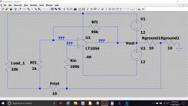
This is a DC sim but the load at the left could equally be a cap where the current in it varies due to either ripple on the rails or the rails being modulated by the audio.
The output of the amp should be 0.00 volts at all times. If you snip the load out of circuit you will get 0V output.
The 10 ohm resistors represent wiring and print resistance.
Now make a two channel version running off one power supply and ensure that where the two input grounds couple together at the audio source that there is also no interaction as one channel draws current and the other does not.
Try cutting the Rf2 ground and now link it back to the junction of V1 and V2. You will get a different result again.
So you have to ensure that your scheme is not influenced by currents flowing in conductors and print. In practice this means ensuring the speaker return comes back to the power supply and that signal grounds (that become a point of reference) are taken from past this high current return.
In the simulation you can also think where any load currents might be returned to such that they do not influence the output voltage. So add a load of say 1k and return it to different ground points and arrange it so that it has no effect. Set a DC input voltage to test this and compare no load vs with a load output voltages.
If you alter the supply voltages, the output voltage should of course be constant. If its not its because the DC currents flowing in the conductors is influencing the voltages seen by the opamp inputs.
Attachments
The power stage and power supply smoothing electrolytic capacitors are on one PCB. This is the original amplifier PCB. The signal processing stages, SMD circuitry, was sawed off. The tracks connecting the output transistors to the supply rails are from the original PCB. These are very thick tracks similar to those found in switching power supplies.
The PCB I built that contains the input, VAS and output protection circuitry takes power from a point near the electrolytic capacitors. The current it draws is very small: 2.5mA for the input stage and 14.5mA for the VAS. This means, it only takes a current that is less than 20mA.
What you, Mooly, illustrated has been on my mind since I started this project. From an engineering point of view, it doesn't make sense to power a circuit from a point where its performance is compromised.
At this point, I am tempted to build a small PCB to host a differential input with equal gains for both the non-inverting and the inverting input. The aim is to have an XLR input. These days, there are audio cards that provide XLR outputs, therefore it makes sense to make an XLR input. The choice is either using a descrete circuit or an integrated circuit.
P.S.
On these fora I found someone posted an XLR input using an instrumentation amplifier. I will opt out of that and use a single op-amp to keep the input impedance down to acceptable values. Very high input impedances seem to have their problems.
Last edited:
I can use INA134 chip to add an XLR input to my amplifier. Besides this is cheaper to implement, the chip is specifically designed for this purpose.
Something like that would give good rejection. There is one minor disadvantage to a simple circuit like this and that is the input impedance is different for each input. Yours would have a 25k and 50k for each input.
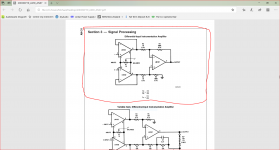
National Semiconductor AN31-9 Section 3
There was an article based on National Semiconductor AN31-9 Section 3 that was published in Audio Amateur or it's successor probably about 20 years or more ago. I have disposed of most of my issues of these publications.
From memory the author used TL072 op.amps in a project to replace a simple pre-amp designed by Marshall Leach.
It was thought to be a step up in sound quality. While the design could be used for hot and cold inputs - I think the latter was connected to earth as a reference point to obtain the claimed improvement.
I used this simple circuit to simulate an XLR input rejecting a 500Hz interference signal. The proper signal frequency is 2000Hz.
There was an article based on National Semiconductor AN31-9 Section 3 that was published in Audio Amateur or it's successor probably about 20 years or more ago. I have disposed of most of my issues of these publications.
From memory the author used TL072 op.amps in a project to replace a simple pre-amp designed by Marshall Leach.
It was thought to be a step up in sound quality. While the design could be used for hot and cold inputs - I think the latter was connected to earth as a reference point to obtain the claimed improvement.
Attachments
- Home
- Amplifiers
- Solid State
- My attempts at a design of a 3 stage amplifier