Taking Andrew T's challenge, I'm posting this experimental variant of JLH's 10W.
The concept is as follows:
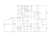
Use D.C. coupled output - needs diff. input pair.
Use current mirror (now standard practice in one form or another)
Output stage: this is where the unusual bit is. The main issue with the original design is that the base current increase in one half can only be provided by a decrease in the other. Because the current gain in an output transistor of the old days falls quite dramatically with current, the increase in current in one half is not the same as the decrease in current in the other. So the average quiescent current had to be set higher.
To remedy this, local feedback is needed. That takes the form of (a) a medium value emitter resistor in the output (b) a driver transistor with medium base resistor too and (c) a 1k bias resistor which sets the current and input impedance, largely.
The voltage amplifier stage uses a standard JLH design in keeping with the original, with CCS load and CCS bias. This is the second unusual bit. In order to bias the output stage, the 1k resistors need a voltage drop of about 1.8V each. So the CCS which starts at 10mA drops after the upper output resistor to 8mA and then again to 6mA for the lower stage. To ensure that the lower stage does not then upset the balance, a CCS stage is used to shunt the excess current. That is fed by a second CCS stage from the top rail but could also be set from the ground rail.
The bias current can be adjusted by altering the current in this second CCS by making R6 a variable (with limiting resistor in series of course).
HF compensation is done with a global compensation capacitor and additional RC phase delay C3 R23.
The PSU voltages are 22V for 16W output.
THD at 1kHz is 0.003% but rises to 0.04% at 20kHz at 10W using epi 2N3055's.
DIY-ers are welcome to make suggestions to improve as I have not built and tested this yet. At 900mV input, another key point is that no transistor cuts off up to at least 200kHz. I think that will eliminate any practical possibility of transient or slew distortion.
The concept is as follows:
Use D.C. coupled output - needs diff. input pair.
Use current mirror (now standard practice in one form or another)
Output stage: this is where the unusual bit is. The main issue with the original design is that the base current increase in one half can only be provided by a decrease in the other. Because the current gain in an output transistor of the old days falls quite dramatically with current, the increase in current in one half is not the same as the decrease in current in the other. So the average quiescent current had to be set higher.
To remedy this, local feedback is needed. That takes the form of (a) a medium value emitter resistor in the output (b) a driver transistor with medium base resistor too and (c) a 1k bias resistor which sets the current and input impedance, largely.
The voltage amplifier stage uses a standard JLH design in keeping with the original, with CCS load and CCS bias. This is the second unusual bit. In order to bias the output stage, the 1k resistors need a voltage drop of about 1.8V each. So the CCS which starts at 10mA drops after the upper output resistor to 8mA and then again to 6mA for the lower stage. To ensure that the lower stage does not then upset the balance, a CCS stage is used to shunt the excess current. That is fed by a second CCS stage from the top rail but could also be set from the ground rail.
The bias current can be adjusted by altering the current in this second CCS by making R6 a variable (with limiting resistor in series of course).
HF compensation is done with a global compensation capacitor and additional RC phase delay C3 R23.
The PSU voltages are 22V for 16W output.
THD at 1kHz is 0.003% but rises to 0.04% at 20kHz at 10W using epi 2N3055's.
DIY-ers are welcome to make suggestions to improve as I have not built and tested this yet. At 900mV input, another key point is that no transistor cuts off up to at least 200kHz. I think that will eliminate any practical possibility of transient or slew distortion.
Attachments
Darlington output etc
I have copied my post in the 'vanilla' JLH69 thread to here for reference and now posted circuit diagrams etc.
Original text
************************
HI Folks,
I said I would report back on how I got on experimenting with the JLH Class A power amp and using Darlingtons in the output stage.
To set the scene, my day to day amp is a Geoff Moss version of the JLH with a high current capability (the ESL version). I use this one because my monitors (B&W Matrix 80 Mk3) can dip down to about 4 ohms in their impedance curve, which means that a normal JLH will have problems driving it at high levels as it not the most efficient of speakers. This amp has 2 sets of output transistors (MK15003) with 0.1 ohm current balancing resistors. You can find the details of this on the Class A amp website
Having experimented with that quite a bit, I replaced the driver/phase splitter with a Szikla pair having a gain of about 3. The measured distortion dropped by about the same value and to my ears the mid range cleaned up: things like the trailing edges of piano notes seem to just be there. You can 'hear the room' on some recordings which all adds up to me of the amp really controlling the speakers. The bass also was something to die for – gut wrenching. The only stability task was a 47pF from the collector to base of the NPN on the Szikla Pair.
By upping the power rails to +/- 30 volts and increasing the standing current, it gives a comfortable 40 watt and get nice and warm. Distortion is down at about 0.0035% or so. Although I have to admit, I cannot hear the difference below 0.1 % and I think that most people would be the same in a double blind test.
I built 2 mono blocks with separate power supplies in another box. You can see some pictures in post 3497 of this thread.
Ever the experimenter, I decided to try and up the output power a bit – aiming for about 60 to 80 watts and see if the distortion could drop down a bit more, (‘cos I can ) so this is why I had a play with the Darlington output stage, but I made a discrete version as I don’t have TO-3 Darlingtons around. I used the MJ15003 with a BD139-16 in front of it and a 100 ohm resistor across the MJ15003 base to emitter.
The pcb I made can be used for the standard Moss configuration or the S-Pair mod so I tried 4 combinations all with a single output pair and I used the same output transistors for all the tests.
The upper MJ15003 has a hfe of 66 and the lower a hfe of 73 and the power rails are+/- 22volts from a stabilised bench supply (my trusty Skytronics). The heatsinks are really big and get up to about 24 degrees above ambient.
The variants I tried are as follows:
(a) The standard Moss version - baseline configuration for reference
(b) The Moss version with a S-pair driver
(c) Version (a) with a Darlington output
(d) Version (b) with a Darlington output
I measured the distortion for a couple of output voltages: 2.8, which equates to about 1 watt into 8 ohms, and 6.3 volts, which is about 5 watts.
Note that these are all measured values into an 8 ohm dummy load – no simulations in sight.
The results look very promising (for some reason I can't get the formatting right on these figures )
(a) Standard Moss config
O/P volts, Iq, Distortion(%)
2.8, 1.9A, 0.004
6.3, 1.9A, 0.01
(b) Moss version with a S-Pair having a gain of 3X
Vout, Iq, Distortion (%)
2.8, 1.9A, 0.0013
6.3, 1.9A , 0.003
These figures seem about right since we are increasing the open loop gain by a factor of 3 and I would expect the distortion to drop by about the same.
Now the good stuff.
To add the Darlington stage I obviously had to make some adjustment to the current setting circuit as it now has to provide less current to the output stage due to their enormous hfe values, which means that it is under less stress.
Interestingly, I did not have to retune the notch filter in the Radford DMS-4, which implies that there was no discernible phase shift by adding the BD139.
The Darlingtons had a hfe of 7070 for the upper and 9460 for the lower.
(c) Standard Moss config with Darlington output
Vout, Iq, Distortion (%)
2.8, 1.9A, 0.0016
6.3, 1.9A, 0.0036
(d) Moss Config with S-pair and Darlington output
Vout Iq Distortion (%)
2.8 (1 Watt), 2.0A, 0.0007
6.3 (5 Watt), 2.0A, 0.001
This seems good so I carried on a bit.
10V (12.5Watt), 0.0018
11V (15 Watt), 0.0022
12V (18 Watt), 0.0024
13V (16.9 Watt), 0.003
14V (24.5 Watt), 0.008 – onset of clipping
The low power distortion figures for (d) are approaching the limits my equipment which is Viktors low distortion oscillator and a Radford DMS-4. The lower limit is about 0.0003% distortion reading. Viktor's oscillator is at least a decade down on this.
So what about listening: I tried the (d) config and could not hear any difference against my day to day amp I mentioned above. The main thing however, is that it opens the door to some high power outputs since it puts less load onto the driver stage.
The figures seem to imply that the S-Pair, acting as a voltage amp of 3x, drives the output more linearly and the Darlington supplies more grunt to the output stage reducing distortion even more.
So folks over to you, it works albeit a bit fidly. How you do the above on the JLH69 I leave to you – experiment some more yourselves
Best regards.
Mike
Circuit diagrams derived from Geoff Moss' modifications
To give some background to my post above, I have put my circuit digarms into Visio and pdf'd them.
To start off with, bear in mind that the excercise was one of experimentation and wanting to try different driver and (predominantly) different output stages.
Consequently, I split the amp into 2 phyisical parts/boards that are linked by a short (3cm) umbilical cable allowing me to mix n' match easily.
(a) a driver board that can accomodate a standard configuration or a S-Pair driver.
(b) an output board that can accomodate standard single output pair, multiple output pairs (up to 4) or darlington output pairs with their current sharing resistors.
These were the basis of the experiments that seem to work out quite well.
Here are the cicuit diagrams. Some additional components were added to make Geoff Moss's driver board more acceptable to my engineering pedancy - some stopper resistors on the presets and an input shunt resistor to keep the input cap charged
I have to admit that I do like the single input transistor geometry: LTPs bring a plethora of problems that have to got around.
Kind regards
Mike
Attachments
Last edited:
- Status
- Not open for further replies.