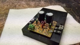
here are gerber files for simple test version if somebody is interested, with all parts and schematic, for power supply +-42V
PCB 5x5cm, price in china PCB service is very cheap - about 8 USD for 5pcs with shipping
PCB 5x5cm, price in china PCB service is very cheap - about 8 USD for 5pcs with shipping
Attachments
Have you compared it to other amps? How does it sound?
Have you measured the voltage at the amps input? is it less than 10mV?
I do not want to underestimate other amplifiers and I prefer other views,
but after listenings in my subjective view this design have now highest priority
")
voltage at inputs is 0mV
I may consider building a CFA with a cascoded voltage gain stage possibly running as a pre amp. Cheers
Have you seen Dadod's preamp?
http://www.diyaudio.com/forums/soli...pre-phone-amp-low-distortion.html#post4826429
No I have never seen it, however I don't like the schematic, the input pair isn't included in the nfb loob, this means the input common collector input is runing without feedback lots of distortion.
Your comment shows your knowledge.
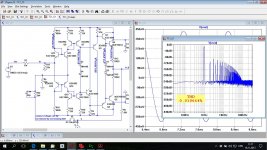
Something even faster - measurements
Sorry but I have to argue that yours is slightly slower than the very fast cfa consept.
In test pictures shown, the 400khz square of very fast is similar to your mosfet 300khz square wave response.
I wanted to comment a bit more on why I don't like the schematic, I revisited the schematic once more, I found out that the input is a common emitter gain stage with current source bias, q11 and q12 acts as each others active load greatly increasing gain, however this collector output of q12 q11 has been shorted to ground by 169ohms this means it goes from a very large gain into a very small gain stage, the input is a cascode, the collectors connect to q3 q4 emiter like a telescopic cascode stage but slightly diffrent. it then drives another cascode gain stage then drives the outputs. The feedback sems to have a dc servo and it goes back to the emiter of q3 q4, at this point q11 q12 collector is also connected, collector cannot act as a feedback point and feeding signals into a collector of a transistor dosen't amplify, the input is running as a zero NFB config. I am supprised that simulation gives very low distriotion.No I have never seen it, however I don't like the schematic, the input pair isn't included in the nfb loob, this means the input common collector input is runing without feedback lots of distortion.
Last edited:
Sorry but I have to argue that yours is slightly slower than the very fast cfa consept.
In test pictures shown, the 400khz square of very fast is similar to your mosfet 300khz square wave response.
Probably need to visit ophthalmologist..
Hi Miro,
I send you some data
Check your mail.
measurements from kct (Kay) and really good listening tests (my and from platon.rado) conviced me to try some improvements ...
today I did first shot with CCS
https://ctrlv.cz/shots/2017/11/17/Obus.png
These symmetric CCS I did:
https://ctrlv.cz/shots/2017/11/17/tEAT.png
https://ctrlv.cz/shots/2017/11/17/CQCq.png
Here is THD:
https://ctrlv.cz/shots/2017/11/17/pgEc.png
AC analysis:
https://ctrlv.cz/shots/2017/11/17/GddL.png
and current drift under working CCS:
https://ctrlv.cz/shots/2017/11/17/W21M.png
https://ctrlv.cz/shots/2017/11/17/g6G3.png
... CCS should be corrected for better values ... but this is only simulation ... if somebody have suggestions from experience? we can match them together ...
I wanted to comment a bit more on why I don't like the schematic, I revisited the schematic once more, I found out that the input is a common emitter gain stage with current source bias, q11 and q12 acts as each others active load greatly increasing gain, however this collector output of q12 q11 has been shorted to ground by 169ohms this means it goes from a very large gain into a very small gain stage, the input is a cascode, the collectors connect to q3 q4 emiter like a telescopic cascode stage but slightly diffrent. it then drives another cascode gain stage then drives the outputs. The feedback sems to have a dc servo and it goes back to the emiter of q3 q4, at this point q11 q12 collector is also connected, collector cannot act as a feedback point and feeding signals into a collector of a transistor dosen't amplify, the input is running as a zero NFB config. I am supprised that simulation gives very low distriotion.
You have to put more effort to understand this amp. Input contains so called supper pairs (Boxall supper pair, sometime wrongly called Baxandall supper pair), it looks similar to the diamond buffer here. The 169R resistor (R19) is a part of NFB together with 470R (R12), and no cascode in the input, just in its output and in the output buffer.
This preamp use about 45 dB of GNFB and open loop gain (about 55 dB) is defined by ratio (R48/R19)*(R5/R15). I hope it will help you.
Don't be surprised with very low distortion.
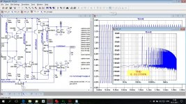
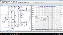
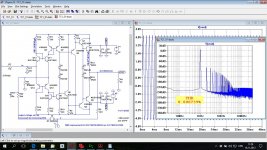
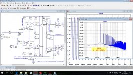
Schematic in post #62 in my opinion use same strange resistor values and very low OPS question current. Attached my simulation. There is quite high crossover distortion and very low input impedance.
Damir
Damir
Attachments
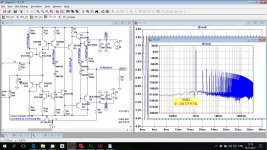
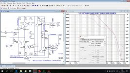
Just by decreasing values for R14 and R16 from 680k (very strange high value) to 47k shows much better results, but still very low input impedance not suitable for some preamps.
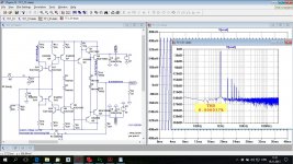
By the way, parallel capacitor(C14) to feedback resistor is not recommended in CFA.
Damir
By the way, parallel capacitor(C14) to feedback resistor is not recommended in CFA.
Damir
Attachments
Just by decreasing values for R14 and R16 from 680k (very strange high value) to 47k shows much better results, but still very low input impedance not suitable for some preamps.
By the way, parallel capacitor(C14) to feedback resistor is not recommended in CFA.
Damir
Damir, as always good and helpfull work.
Thank you also for this usefull information.
Could you please, share the simulation file?
Thank you.
- Status
- This old topic is closed. If you want to reopen this topic, contact a moderator using the "Report Post" button.
- Home
- Amplifiers
- Solid State
- Another very fast CFA concept