Member
Joined 2009
Paid Member
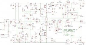
I got tempted to build a clone of a NAIM amplifier.
There are various schematics floating around and I don't think there's a definitive one I can point to. Searches for 'NAP 140' turn up some good starting points.
I've attached what I believe is the popular approach muddied somewhat by my ad-hoc part numbering. I added my own dc-speaker protection circuit with solid-state relay.
I'd really appreciate a sanity check and comments on possible errors. The NAIM circuits appear to have a reputation for h.f. instability and Spice simulations seem to confirm some 'interesting' behaviour out past the audio spectrum.
p.s. A thank you is owed to Brian 'Traderbam' for some helpful comments (offline) that has got me to this point.
Attachments
Last edited:
Schematic looks wrong in CCS for TIS/VAS. There is no resistor to set Iq for this stage.
Original VAS/TIS runs approximately 10mA, so the Pc of TR6 may over, try to change it by Zetex devices.
Original VAS/TIS runs approximately 10mA, so the Pc of TR6 may over, try to change it by Zetex devices.
Member
Joined 2009
Paid Member
I reverse engineered this pcb, from an original NPA 110.
Yes, indeed there is 68R resistor in the emitter circuit for the VAS current sink. I'll add that in.
Note that I leave out the SOAR protection circuit altogether.
Also, I have made a small modification to the Vbe multiplier circuit for proper tracking. The original Naim relied on ambient air temperature inside a closed box to thermally couple the Vbe multiplier to the driver of the Sziklair output pair at the -Ve rail. As designed, the Vbe multiplier is too sensitive for direct physical coupling to the output stage. My modification allows direct coupling at the appropriate level of sensitivity - I feel safer this way.
Some parts values on the photo don't match my schematic - will have to investigate further.
Attachments

Last edited:
The pcb execution has elements that are undisclosed part of the circuit.
Julian Vereker had a software designer devise a program that could produce the curves evident on the pcb with varying widths and radii and model the effects of the overall design.
The better clones of this circuit copy the exact layout of the Naim pcb.
Julian Vereker had a software designer devise a program that could produce the curves evident on the pcb with varying widths and radii and model the effects of the overall design.
The better clones of this circuit copy the exact layout of the Naim pcb.
Yes, the bias circuit of original Naim that not good. When amplifier hot, the bias will increase. The incorrect position of 27R and the distance of BIAS transistor are the problem.
I have only change position of that resistor and mounting it to heatsink => the problem is solved.
I have only change position of that resistor and mounting it to heatsink => the problem is solved.
I believe there are phase shift networks in parallel with the output device stoppers...... unique quality to Naim that Vereker talks about, though obliquely. He insists that most of the ideas were not his, but unearthed from study of work of others.
Hugh
Hugh
Member
Joined 2009
Paid Member
The pcb execution has elements that are undisclosed part of the circuit.
Julian Vereker had a software designer devise a program that could produce the curves evident on the pcb with varying widths and radii and model the effects of the overall design.
The better clones of this circuit copy the exact layout of the Naim pcb.
If that's what somebody told you then it sounds like a huge bunch of old codswallop to me 😛
Sure, there will be inductance and capacitance variations with pcb design but if you think about it, there is simply no sense in trying to reproduce an exact NAP as there are too many things you can't duplicate. I don't want to use 40 year old electrolytic capacitor technology in my power supply for starters and modern transistors are produced using modern semiconductor processes - the old ones simply aren't available.
Nevertheless, I've read quite a few threads on different forums of late and there are an awful lot of folk interested in building clones or modifying / repairing old Naim gear. It seems a great deal of fun to me and if we don't get too anal about it all there is plenty of scope for a great amplifier which likely has some flavour of the Naim heritage however you choose to look at it

Member
Joined 2009
Paid Member
I have only change position of that resistor and mounting it to heatsink => the problem is solved.
That's good to know, always nice when the theory turns out to work in practice.
I believe there are phase shift networks in parallel with the output device stoppers...... unique quality to Naim that Vereker talks about, though obliquely.
I don't really understand why he added these networks, or how they help with the stability of the amp, or how the parts values are optimized.
If that's what somebody told you then it sounds like a huge bunch of old codswallop to me 😛
Occasionally Julian Vereker granted Q & A interviews to Hi-Fi journalists. There is a body of well informed opinion in the field of audio electronics - so if some claim does not stack up it will come under fire.
Apart from that there is the matter of a business case to justify the software development costs - it is no different from automated production.
If a small package transistor gets hot through running 10 m.a. ask yourself why has a decision been made to transfer the heat through the leads to the pcb copper and why is the bias transistor not fixed to the main heat sink.
To understand what this is about requires some thinking outside the square. I challenge you to do that.
You might find it interesting to look at details and discussion of another popular revamped Naim design called HackerNap, from a few years ago: https://app.box.com/s/jnasoijb2gg7mopasbuo/1/128283763
Like just about all serious UK Naim tweaking, it has its origins in threads at the PFM forum.
BTW, Nap 110 has lower rail voltages and consequently different bias setting resistors in the front end.
Like just about all serious UK Naim tweaking, it has its origins in threads at the PFM forum.
BTW, Nap 110 has lower rail voltages and consequently different bias setting resistors in the front end.
Last edited:
That's a solution for the general problem with thermal compensation for any quasi-complementary design. If you use the heatsink as the reference temperature it won't track the bias correctly - often resulting in a fire-prone amp unless very low bias is used. A common solution is to use the air in the case somewhere near the heatsink but not on it, just as Naim does. As discussed and referenced in the other thread, exact bias for a quasi' doesn't really make much practical difference anyway - it can only offer a compromise of bias current and thermal coefficients that don't encourage thermal runaway.....why is the bias transistor not fixed to the main heat sink.....
Member
Joined 2009
Paid Member
I wonder whether it was cheaper for him to get somebody to do that instead of buying something off the shelf - I'm not very familiar with what the 70's had to offer in terms of software?... there is the matter of a business case to justify the software development costs - it is no different from automated production.
If a small package transistor gets hot through running 10 m.a. ask yourself why has a decision been made to transfer the heat through the leads to the pcb copper and why is the bias transistor not fixed to the main heat sink..
+1
I was mulling over the thermal situation last night after your original post got me thinking. I'm not sure my compact pcb allows for this and I'm going to consider gluing a copper fin onto the transistor to help it shed some heat. Those E-line packages aren't so common but I read that Naim was happy with these devices running quite warm.
Member
Joined 2009
Paid Member
That's a solution for the general problem with thermal compensation for any quasi-complementary design.
I don't understand why quasi temperature comp. is an issue here - no prior experience on my part though.
The -ve feedback loop has unity gain at DC, it will servo the output to close to zero volts. So if the output idle current starts to change through either the Darlington (+ve rail) or Sziklai (-ve rail) outputs this dc servo action will balance the two outputs to ensure zero output. This means you have only to put a thermal servo on one output to control it. The complication, if it is one, is that the Darlington thermal servo should be based of the main heatsink whereas the Sziklai is often servoed from the driver device. But in the quasi, the main heatsink is perfectly valid too. Is it not ?
Last edited:
DC protect
The 200 Volt Fets used in the DC protection have a very high Rdson about 190 mOhms in series . This has serious impact on the damping factor of the amp . 100 Volt Fets would be Ok here and they are widely available in less than 10 mOhm Rdson .
Cheers ,
Rens
The 200 Volt Fets used in the DC protection have a very high Rdson about 190 mOhms in series . This has serious impact on the damping factor of the amp . 100 Volt Fets would be Ok here and they are widely available in less than 10 mOhm Rdson .
Cheers ,
Rens
Member
Joined 2009
Paid Member
Thanks Rens, I will look into that.
Interestingly, the NAP 140 is designed with an 0R22 resistor at the output, perhaps the Rdson of the FETs is desirable for this project.
Interestingly, the NAP 140 is designed with an 0R22 resistor at the output, perhaps the Rdson of the FETs is desirable for this project.
I wonder whether it was cheaper for him to get somebody to do that instead of buying something off the shelf - I'm not very familiar with what the 70's had to offer in terms of software?
+1
I was mulling over the thermal situation last night after your original post got me thinking. I'm not sure my compact pcb allows for this and I'm going to consider gluing a copper fin onto the transistor to help it shed some heat. Those E-line packages aren't so common but I read that Naim was happy with these devices running quite warm.
On the first point I think the time would more likely have been in the 1980's. It could have been that JV bought software packages off the shelf and asked developers to customise these to his needs.
Running the E-line packages at elevated current levels has advantages in terms of current gain (which increases with temperature) and Miller capacitance.
Also the stage voltage gain is in proportion to the collector current - roughly 40 per m.a. times the collector load in k ohms.
Understanding heat will migrate via the transistor leads, I see the pattern area of copper on the underside of the board as having to do with a temperature sweet spot as well as adding some capacitance between the leads.
If a copper fin is glued to the flat face of an E-Line transistor the effect of the intimate contact on junction capacitance is indeterminable.
Together with your more compact layout this may work satisfactorily however there are some subtle aspects in the original design that I would not write off as totally immaterial.
It may be useful to measure the temperature of the Vas transistor in the Naim unit and match the heat sink size for your design to deliver the same result.
If a copper fin is glued to the flat face of an E-Line transistor the effect of the intimate contact on junction capacitance is indeterminable.
In the sense that does not count and therefore does not compensate for whatever is allowed for in the pcb track layout.
Member
Joined 2009
Paid Member
I don't have access to an original Naim to compare with - I'm driving in the dark and you guys are my eyes.
The junction capacitance will be dominated by the intrinsic VAS Cob and Cdom so the pcb parasitics should be negligible ?
The one thing that bothers me the most is the h.f. aspects. I don't understand the premise behind the phase-networks (as Hugh calls them) in parallel with the driver base-stoppers and how to optimize the part values for modern output devices (with their superior beta-droop and higher fT's).
I also don't know if the phase lead compensation network across the feedback resistor needs adjustment. I will at least be able to look at a square wave test signal on a sillyscope for signs of trouble but in simulations I didn't get satisfaction.
p.s. I wonder how much we are 'reading' into the old Naim pcb layouts. The NAP 110 looks remarkably like the kind of layout a hobbyist might come up with if they were trying to start up a small business and simply trying to translate a rudimentary schematic onto a pcb where they were going for a single sided design for etching in the kitchen sink.........
Last edited:
Although after many years of listening to Naim clones my interest in that subject is somehow dininished, I will add a few comments to Biguns interesting project (please excuse my english in case of misunderstandings):
Here is a scan of a photo of the NAP 250 power amp stage from the chrome bumper age - without the regulators; for those who are new to this subject: The NAP250 had a fully regulated power supply individually for both channels:

Since Biguns schematic (in the basic outline) is closer to the original than the dreadful Avondale clone schematic, it is interesting how simple the original schematic is. (f.e. Instead of Avondales claims the input differential pair has no degeneration resistors, etc.)
It is definitely a tweaked design, which relates heavily to the exact parts (a perhaps matchings). Grounding is important, as always with Naim designs, but the exact PCB layout is simple and clear, without any magic track lenghth or the like.
I am referring to Biguns parts number here.
Please note the the main star ground is directly connected to the input ground (the green wire), no R2 (10R) here. The feedback ground and the input ground meet at a central (star) spot.
No antiparallel diodes across the feedback cap.
Exept of the input transistors (BC239 selected, usually marked) all other small signal transistors are e-line, that means ZTX753/653 for the drivers and - as far as I can remember - ZTX453 for the input CCS. Maybe that was another ZTX653, it seems not so critical here. Other Naim amps had different transistors here too (MPSA18 or 06).
The current control circuit uses ZTX453 etc. but is not used with Biguns circuit. I also always did the same - with some attention I did not need it. But the NAP250 amplifier was always also used with very difficult loads like Quad electrostatics and also could survive a short "short". Without the over-current circuit it wont.
The bias transistor was another ZTX653, which is not critical here. Interestingly this transistor is not mounted on the heatsink, as one should estimate, but right in the middle of the board, thus only coupled by the air temperature. But the closed non-ventilated Naim case was actually a big heatsink itself, so the inside temperature was pretty even, I guess.
The driver transistors were MJE340/350 as far as I can remember, but I will look into my texts tomorrow again.The baxandall diode is a normal 1N4148.
The power transistors are custom made for Naim (in those days by Semelab) and it is said that they are equivalent or similar to the BUV20, a fast switching transistor. Julian Vereker said in at least one interview, that he wanted a fast, but not necessary super linear transistor to work in a relativly low biased Class AB amp.
In the last remaining Naim clone I have I use the PT77 (by ST), a mil-spec version, originally made for the Cyrus 2. I do not recall the equivalent type at the moment.
The power emitter resistors, are Welwyn wirewound 0.22R, as wall as the 8R resistor for the output zobel. There is another output resistor with again 0.22R in line of the output, to linearize the damping factor for the full spectrum (at a lower but frequency constant level) and to isolate the output from the feedback line. This resistor is the most hated component and is omitted in most of the clones, but is mandatory for all Naim amps. (Maybe not until today, but today's version of these amps are not so interesting anymore...).
Instead of the output inductor Naim uses that 0.22R output resistor and recommended at least 2m lenghth of low capacitance loudspeaker cables. Their inductivity provided enough stabilty to the amp.
Interestingly all the resistors are pretty basic metal film types with 5% tolerance, except for the feedback resistors.
The caps are styroflex and tantalum beads, even the feedback cap and the input cap are polarized. The feedback cap had only 68uF.
I guess that the compensation R-C parts are tuned to the parts, they are different in other Naim amps, the Nait (1 and 2) did not have any. Of course all the Naim amps have the compensation R-C parts over the feedback resistor to shape the transient behaviour of the amp.
More later, also some more component values, if interested. It is late today here. I hope I can support this project. (Although I would never put those mosfets into the output line.)
Unfortunately, and I have said that already long ago here in one of the many Naim threads, I have never heard a Naim clone, which sounded better than the original ones. Not even mine.
I do not know why that is so, but I will stand corrected if that is not true and am looking forward to the first one which does. As an excuse I want to mention that I knew much less about amplifiers in the eighties than I know now (beeing involved in the NERO/Nytech resourrection...).
Here is a scan of a photo of the NAP 250 power amp stage from the chrome bumper age - without the regulators; for those who are new to this subject: The NAP250 had a fully regulated power supply individually for both channels:
Since Biguns schematic (in the basic outline) is closer to the original than the dreadful Avondale clone schematic, it is interesting how simple the original schematic is. (f.e. Instead of Avondales claims the input differential pair has no degeneration resistors, etc.)
It is definitely a tweaked design, which relates heavily to the exact parts (a perhaps matchings). Grounding is important, as always with Naim designs, but the exact PCB layout is simple and clear, without any magic track lenghth or the like.
I am referring to Biguns parts number here.
Please note the the main star ground is directly connected to the input ground (the green wire), no R2 (10R) here. The feedback ground and the input ground meet at a central (star) spot.
No antiparallel diodes across the feedback cap.
Exept of the input transistors (BC239 selected, usually marked) all other small signal transistors are e-line, that means ZTX753/653 for the drivers and - as far as I can remember - ZTX453 for the input CCS. Maybe that was another ZTX653, it seems not so critical here. Other Naim amps had different transistors here too (MPSA18 or 06).
The current control circuit uses ZTX453 etc. but is not used with Biguns circuit. I also always did the same - with some attention I did not need it. But the NAP250 amplifier was always also used with very difficult loads like Quad electrostatics and also could survive a short "short". Without the over-current circuit it wont.
The bias transistor was another ZTX653, which is not critical here. Interestingly this transistor is not mounted on the heatsink, as one should estimate, but right in the middle of the board, thus only coupled by the air temperature. But the closed non-ventilated Naim case was actually a big heatsink itself, so the inside temperature was pretty even, I guess.
The driver transistors were MJE340/350 as far as I can remember, but I will look into my texts tomorrow again.The baxandall diode is a normal 1N4148.
The power transistors are custom made for Naim (in those days by Semelab) and it is said that they are equivalent or similar to the BUV20, a fast switching transistor. Julian Vereker said in at least one interview, that he wanted a fast, but not necessary super linear transistor to work in a relativly low biased Class AB amp.
In the last remaining Naim clone I have I use the PT77 (by ST), a mil-spec version, originally made for the Cyrus 2. I do not recall the equivalent type at the moment.
The power emitter resistors, are Welwyn wirewound 0.22R, as wall as the 8R resistor for the output zobel. There is another output resistor with again 0.22R in line of the output, to linearize the damping factor for the full spectrum (at a lower but frequency constant level) and to isolate the output from the feedback line. This resistor is the most hated component and is omitted in most of the clones, but is mandatory for all Naim amps. (Maybe not until today, but today's version of these amps are not so interesting anymore...).
Instead of the output inductor Naim uses that 0.22R output resistor and recommended at least 2m lenghth of low capacitance loudspeaker cables. Their inductivity provided enough stabilty to the amp.
Interestingly all the resistors are pretty basic metal film types with 5% tolerance, except for the feedback resistors.
The caps are styroflex and tantalum beads, even the feedback cap and the input cap are polarized. The feedback cap had only 68uF.
I guess that the compensation R-C parts are tuned to the parts, they are different in other Naim amps, the Nait (1 and 2) did not have any. Of course all the Naim amps have the compensation R-C parts over the feedback resistor to shape the transient behaviour of the amp.
More later, also some more component values, if interested. It is late today here. I hope I can support this project. (Although I would never put those mosfets into the output line.)
Unfortunately, and I have said that already long ago here in one of the many Naim threads, I have never heard a Naim clone, which sounded better than the original ones. Not even mine.
I do not know why that is so, but I will stand corrected if that is not true and am looking forward to the first one which does. As an excuse I want to mention that I knew much less about amplifiers in the eighties than I know now (beeing involved in the NERO/Nytech resourrection...).

The phase compensation networks - as JV called those himself - he copied from early Spectral amplifiers and tuned them by ear, as he said. We should do the same.
The feedback compensation network can also be tuned by ear also, 39pF is the original value in the NAP250, a higher value makes the amp more slow, mellow and much darker sounding.
The feedback compensation network can also be tuned by ear also, 39pF is the original value in the NAP250, a higher value makes the amp more slow, mellow and much darker sounding.
- Status
- Not open for further replies.
- Home
- Amplifiers
- Solid State
- TGM10 - based on NAIM by Julian Vereker