Together with your more compact layout this may work satisfactorily however there are some subtle aspects in the original design that I would not write off as totally immaterial.
It may be useful to measure the temperature of the Vas transistor in the Naim unit and match the heat sink size for your design to deliver the same result.
I second both aspects.
I do not think that there is some magic involved, but we should not overlook seemingly uninportant spots in that circuit.
The VAS transistor is somewhere close to the input pair, but that can also be purly incidental by some layout settings.
Bigun, do you really think you can adjust the offset by adjusting the ccs for the input differential pair?
I remember discussions over now decades why the Naims must be bad. Mainly because some people did not like the circuit design, or some parts of it. Mostly the output resistor.
But is is a design which shows the value of synergy. Let us finally find out how. The Amps sound very very good indeed, in their own autonomous manner, if you like.
But is is a design which shows the value of synergy. Let us finally find out how. The Amps sound very very good indeed, in their own autonomous manner, if you like.
Member
Joined 2009
Paid Member
Hi Lohk, great to have your contributions !
they are only included in case the amplifier fails and stresses the caps but I guess if I were worried I could use a bipolar cap of decent voltage headroom - diodes are gone !No antiparallel diodes across the feedback cap.
I’ve never felt the need to use one they have a bad reputation for their adverse impact on the sound quality of the amplifier.Without the over-current circuit …
the photo I have of a NAP 110 shows a mix of E-line and TO-92.Exept of the input transistors (BC239 selected, usually marked) all other small signal transistors are e-line
I figure that the 2SC5200 would be a nice option. I have some on hand which always helps.The power transistors are custom made for Naim … Julian Vereker said he wanted a fast, but not necessary super linear transistor
good to know, I’m going to try and find them or equivalent.power emitter resistors, are Welwyn wirewound 0.22R, as wall as the 8R resistor for the output zobel.
I don’t worry about that, I’m building for the fun of building and for learning something new about a famous amplifier. If I was really wanting a NAP 140 there are plenty around for a few hundred dollars and they are re-sellable so you get to ‘rent’ one for far far less than it’s going to cost to build a clone. Hmmm, now that I think about it…Unfortunately, and I have said that already long ago here in one of the many Naim threads, I have never heard a Naim clone, which sounded better than the original ones. Not even mine.
what would we be listening for in terms of the sound ? I have heard the impact of varying Cdom just exactly as you describe. Is it the same with the phase compensation networks on the driver bases ?The phase compensation networks - as JV called those himself - he copied from early Spectral amplifiers and tuned them by ear, as he said. We should do the same.
is this not a common method?Bigun, do you really think you can adjust the offset by adjusting the ccs for the input differential pair?
Last edited:
Gareth,
For your mosfet `speaker relay' I think either the FDP083n15a or irfi4228pbf would be better - much lower Rdson.
I like the idea of leaving off the output short circuit protection, as I don't think the NAIM circuit works very well. Even with the latest NAP300, the protection circuit can occasionally be heard working when it shouldn't, especially with the new Focal Sophia 2 speakers (though they do sound good together most of the time).
Also I think R1B is a bit high at 4.7k, I'd make it 1k.
Regards,
Paul Bysouth
The one thing that bothers me the most is the h.f. aspects. I don't understand the premise behind the phase-networks (as Hugh calls them) in parallel with the driver base-stoppers and how to optimize the part values for modern output devices (with their superior beta-droop and higher fT's).
I also don't know if the phase lead compensation network across the feedback resistor needs adjustment. I will at least be able to look at a square wave test signal on a sillyscope for signs of trouble but in simulations I didn't get satisfaction.
Q8 the pnp driver transistor has a collector load resistor of 100R the corresponding npn driver transistor has no collector load.
The presence of a load in the pnp collector circuit has an impact on the width of the depletion layer between the collector and the base which depends on the voltage applied to the collector.
The capacitance developed between the collector and base will be lower when the applied voltage is at it's highest value and greatest when the applied voltage is at the lowest value - i.e. when the drop across the 100R resistor is greatest. There will be a little bit of Miller effect there as well.
From this you can conclude there is going to be a lag in the response of the pnp driver transistor.
The bypass lead arrangements in each the input of each output half are to compensate for this so both output halves are in reasonable phase alignment - as pointed out by JV - in that way the negative feedback loop will be more effective.
If you want to avoid the vagaries of experimenting with different driver transistors you could use MJE243 and MJE253 devices. You can make out the part numbers from the recent photo by enlarging the image.
Member
Joined 2009
Paid Member
The bypass lead arrangements in each the input of each output half are to compensate for this so both output halves are in reasonable phase alignment - as pointed out by JV - in that way the negative feedback loop will be more effective.
oh this is fascinating, I've never seen this mentioned anywhere, in any book or internet site, amplifier description or otherwise. I shall give this some thought!
I can see pcb parasitics and specific device choices making some difference. It is also consistent with JV wanting to have very fast output devices even at the expense of their linearity.
On the face of it, I don't fancy trying to tune those circuits by ear. A sillscope and open-loop amplifier would seem a far better approach, temporarily substituting a small variable resistor and watching the output.
Last edited:
Member
Joined 2009
Paid Member
how does it sound compared to say aksa? Cuz it looks like aksa+ ccs
These amplifiers are so different from each other I'm not sure I know where to start. The CCS feed for the LTP prevents supply rail modulations by the signal from mixing with the input & feedback signals (Gilbert cell), the CCS load for the VAS behaves differently than a bootstrapped VAS, phase lead compensation inclusive of the output stage in one case, of the VAS in the other, different feedback networks, different philosophy for emitter load resistors at the output and different base stopper networks on the drivers, low Cob vs higher Cob VAS devices, Quasi vs complementary. etc. etc. etc. I will have a chance to listen to my clone of each but that's not the same as comparing the originals of course.
A few more details, which I have not mentioned yet:
Behind the supply wires there is the zobel cap hidden (100nF, MKP) and the second ground wire for the zobel (green). The red one is the obvious positive supply wire and the black negative one is barely visible. Also hidden behind those wires there are two diodes, parallel and close to the output transistors in inverse polarity. Naim used FR105 diodes here, as far as I can remember, fast diodes as safety for the fast transistors and to suppress the switching spikes to reduce output distortion, I assume.
One of the things people seem to hate with these amps are the tantalum caps in the signal and feedback path. Many people, professional designers as well as diyers seem to avoid that like the devil shyes holy water. But strangely again: the amps sounded good - nevertheless.
Interestinglythere were no stabilizing caps on the power amp board, not even the minimum foil-caps. The only caps on the regulated rails are a Philips BC elcap with 10uF/63V on every power supply output, situateted on the power supply boards.
The star ground for the whole amplifier is at/between the minus output sockets.
I will post some more images and details later, I promise.
Member
Joined 2009
Paid Member
Behind the supply wires there is the zobel cap hidden (100nF, MKP)
If you look at the image in post #3 you can see the zobel cap quite clearly on the NAP 110.
Some corrections:
In my remaining "Naim clone" - something between a NAP180 and a NAP110, in double mono layout, I use BC182C for the input pair and ZTX 452/552 for the VAS and the subsequent CCS. Driver transistors are MJE243/253. The feedback cap has only 47uF/6.3V.
I remember having seen all those in real Naim amps.
Member
Joined 2009
Paid Member
This is important because the pin-out of the TO-92 parts varies a lot between types (sometimes between brands of same time). The E-line parts seem to me to be consistent in their pin-out e-b-c (looking from top/front) and so are TO-126 devices which are consistently e-c-b (looking from top/front).
The BC546 that are sometimes recommended for the LTP in clones are c-b-e (from top/front) which is what I've used in my layout. Fortunately, the BC182 is also c-b-e (from top/front). I can also install an E-line (ZTX) device into the same pin-out so it should be flexible enough. phew!
What's interesting is that the photo in post #3 of a NAP 110 shows a TO-92 device in place for the VAS ?
Last edited:
That is interesting. But the NAP110 you have posted is one of the oldest ones I have ever seen. With the original Naim transistors from the 70ies!
Here is an image of the psu regulator:

and another one of the main psu:

Here you can see the star ground.
Please note that most of the Naim amps used full-wave rectification, the 500VA transformer has two centertapped windings and the two bridges use only two diodes per voltage side.
I remember haven compared that layout (together with some friends way back in the eighties) to a full- bridge rectification, but we all liked the full-wave setting much better. Maybe less diode/switching noise?
and another one of the main psu:
Here you can see the star ground.
Please note that most of the Naim amps used full-wave rectification, the 500VA transformer has two centertapped windings and the two bridges use only two diodes per voltage side.
I remember haven compared that layout (together with some friends way back in the eighties) to a full- bridge rectification, but we all liked the full-wave setting much better. Maybe less diode/switching noise?
Member
Joined 2009
Paid Member
I shall place a star ground on the pcb. There will be two rail capacitors (4,700uF per cap) per rail on the pcb with provision for a wire link or resistor between them so I can have a CRC on-board if desired. Each rail cap will return a ground trace to the star point. The front end of the amplifier also has decoupling capacitors which will also have traces back to the star point. The zobel cap will return there too.
The signal ground will be separated, just like the NAP110. I will provide a place for a wire link or resistor to connect the signal ground to the star ground if desired.
The signal ground will be separated, just like the NAP110. I will provide a place for a wire link or resistor to connect the signal ground to the star ground if desired.
maybe off topic:
Part of the Naim sound also results from the preamps, which are, or at least were, fabulous and I am still using a NAC42. All capacitor coupled single ended Class-A designs and can be tweaked "in all directions".
Part of the Naim sound also results from the preamps, which are, or at least were, fabulous and I am still using a NAC42. All capacitor coupled single ended Class-A designs and can be tweaked "in all directions".
Bigun, I am looking forward to your results.
Maybe I should make another "clone" after all those years, but there are so many other projects pending... It has been posted that much in this forum and others about that amps, that I sometimes mix up details. But the issue why these amps have their special sound was never really solved. It must be a mix of the mentioned parts and tweaks, and this topology (the un-balanced input stage, the VAS, or whatever). Knowledgable specialists like Ian Finch or Hugh Dean from AKSA will bring even more input here, I hope.
Maybe I should make another "clone" after all those years, but there are so many other projects pending... It has been posted that much in this forum and others about that amps, that I sometimes mix up details. But the issue why these amps have their special sound was never really solved. It must be a mix of the mentioned parts and tweaks, and this topology (the un-balanced input stage, the VAS, or whatever). Knowledgable specialists like Ian Finch or Hugh Dean from AKSA will bring even more input here, I hope.
What's interesting is that the photo in post #3 of a NAP 110 shows a TO-92 device in place for the VAS ?
Indeed! Quite possibly the part used there is BC640 which has a very high Early voltage factor (VAF =144) and high current gain (BF=185)as seen in the Siemens SPICE file.
.MODEL BC640/SIE PNP
+ AF= 1.00E+00 BF= 1.85E+02 BR= 4.28E+00 CJC= 8.00E-11
+ CJE= 1.27E-10 CJS= 0.00E+00 EG= 1.11E+00 FC= 5.00E-01
+ IKF= 9.69E-01 IKR= 1.00E+00 IRB= 1.62E-01 IS= 4.60E-12
+ ISC= 9.45E-17 ISE= 1.99E-14 ITF= 4.53E-01 KF= 0.00E+00
+ MJC= 5.07E-01 MJE= 4.94E-01 MJS= 3.30E-01 NC= 2.00E+00
+ NE= 1.23E+00 NF= 1.19E+00 NR= 1.23E+00 PTF= 0.00E+00
+ RB= 4.84E+00 RBM= 1.00E+01 RC= 2.62E-01 RE= 1.00E-02
+ TF= 1.07E-09 TR= 0.00E+00 VAF= 1.44E+02 VAR= 1.97E+01
+ VJC= 3.62E-01 VJE= 5.43E-01 VJS= 7.50E-01 VTF= 9.99E+05
+ XCJC= 1.00E+00 XTB= 0.00E+00 XTF= 6.31E-01 XTI= 3.00E+00)
*
Early effect is a phenomenon where the width of the base is affected by the voltage by the voltage applied to the collector in a common emitter amplifier - a common description is base width modulation. It is more of an annoyance if anything but you would minimise the impact if you can.
Member
Joined 2009
Paid Member
"Quite possibly" - are you making a hint because you have seen this part or is this a wild guess ? 😀Indeed! Quite possibly the part used there is BC640
PCB
===
I've imposed a few constraints on the pcb layout which will likely displease many of you 😡
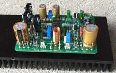
I have some boxes to use for this amplifier with heatsinks drilled and tapped. The power devices need to go where the tapped holes are and the pcb has to fit over the top of them. The good news is that I've already built 3 different amplifiers with these constraints and they all turned out just fine.
Photo is of my last project, TGM1i, essentially the AKSA 100 power amp. I'm going to use the same size pcb so this photo gives a good indication of what I have in mind.
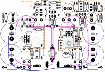
The sketch up I've attached shows where the major items are for my Naim clone layout. Rail caps on each side. Power devices underneath. The drivers with their own heatsinks are placed close to the output power devices. The output inductor and zobel near the centre at the lower edge and the sensitive input circuity at the top edge.
p.s. nice photo of a Naim regulator board above. I'm planning to build one of those (or similar) and make my own version of the Naim Statement amp, a much simpler, much smaller version on the same size pcb as this current project. Like the Naim S-amp it'll be a zero feedback complementary design. It'll go in the last of the metal boxes I have.
Attachments
Last edited:
- Status
- Not open for further replies.
- Home
- Amplifiers
- Solid State
- TGM10 - based on NAIM by Julian Vereker