When did I ask you to tease me? Who gives you the right to do so? This is not facebook. You wasted so much time telling me something unnecessary. I asked how I can limit the current to 2.5A(post 1) at 1ohm(FET intrinsic) load(post 10) and this is what you did, wasted a lot of space-time!!! Please do not ask or suggest anything. I am no longer asking you.
I do not want knowledge on anything other than appropriate values for the Zeners. I know I can figure it out by experimenting. But I thought I could save time by asking here(which is exactly why this site exists for), looks like I wasted that time.
Respectable users, please don't post if you hate this thread. I don't care for your suggestions on how many things I can cut from this circuit or why a LatFET should not be used with external zeners. And if you want to tease me like WuYit then please open a new thread named "Lets Tease Shaan" under The Lounge section.
Have a nice day.
Hi, ilimzn
Thanks for the explanation.
So if the N-ch stopper R is made a bit higher than the P-ch stopper R, is then bypass cap across the bias R not needed?
Thanks for the explanation.
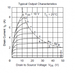
IT should be noted that the discontinuity of Ciss between P and N CH types is still visible regardless of the capacitor due to the gate stoppers, because they limit charge/discharge current. Unfortunately, there is little that can be done against that, as the stoppers are a necessity. On the other hand, there is a different approach, where the crossover notch is 'modified' by the careful choice of gate stopper values.
So if the N-ch stopper R is made a bit higher than the P-ch stopper R, is then bypass cap across the bias R not needed?
Hi Shaan
If you look at the datasheet for 2SJ162 you see that there are internal gate to source diodes. These are for ESD protection of the gate to source junction, since more than 15V between gate and source pins will shoot through the oxide layer and destroy the device. However, a smaller voltage gate to source zener would limit Id by limiting Vgs. for 2.5A, limit Vgs to 4V or so. On the issue of gate stopper and crossover, a gate low pass or Zobel filter right at the device gate pin to GND will allow the use of smaller gate stopper resistor. It is common to use different values for N-ch and P-ch. They are not identically oposite.
If you look at the datasheet for 2SJ162 you see that there are internal gate to source diodes. These are for ESD protection of the gate to source junction, since more than 15V between gate and source pins will shoot through the oxide layer and destroy the device. However, a smaller voltage gate to source zener would limit Id by limiting Vgs. for 2.5A, limit Vgs to 4V or so. On the issue of gate stopper and crossover, a gate low pass or Zobel filter right at the device gate pin to GND will allow the use of smaller gate stopper resistor. It is common to use different values for N-ch and P-ch. They are not identically oposite.
Last edited:
However, a smaller voltage gate to source zener would limit Id by limiting Vgs. for 2.5A, limit Vgs to 4V or so.
This was exactly my point from the start. I wonder how some mature member don't get simple things!
I better try it myself than waste any more time explaining my question! For the time being I am using a 3V3 zener and a 1N4007 in series. So Vgs would be max 3V9 or so.
Now I need to figure out Id at Vgs 3V9 by testing.
Thanks for your kindness CBS240.
I like it. That is the point. I am being an amateur, which I am. Why are you caring. Thanks I don't need foolproof protection. I am not interested.
That aside please stop asking like this as I am no longer interested in it. Or else I will have to report it to the moderators.
Thanks.
That aside please stop asking like this as I am no longer interested in it. Or else I will have to report it to the moderators.
Thanks.
Last edited:
I like it. That is the point. I am being an amateur, which I am. Why are you caring. Thanks I don't need foolproof protection. I am not interested.
That aside please stop asking like this as I am no longer interested in it. Or else I will have to report it to the moderators.
Thanks.
You are basing your calculation wrong, as it's not really based on inherent Rdson. Gate zeners do not provide adequate short circuit protection long term if there are no fuses. The idea is to limit the current through the MOSFETs for long enough to burn the fuses. Thereafter, since you cannot expect both V+ and V- fuses to burn simultaneously, DC may appear and that is taken care of by DC protection.
In your case, the lowish power supply voltage makes it possible for the MOSFETs to last longer under short circuit conditions. Even limiting the current to 2.5A in theory produces 50W dissipation (both MOSFETs together) which is not a trivial amount of heat to dissipate. The negative tempco of the MOSFETs will reduce this as temperature goes up, and although these MOSFETs are very rugged for their ratings, this condition should not last indefinitely, as deterioration will occur. In other words, it will work like you propose but not without problems down the line.
Also, it should be noted that the low power supply voltage quite severely limits output power, by limiting the available current into the load because of limited maximum Vgs you can get. Laterals are particularly problematic here due to low transconductance, so lots of Vgs is required to turn them fully on. In theory, you could get the full 7A through the MOSFET with an output voltage of less than 10V peak, and that's assuming no supply voltage drop as current increases. Unfortunately, this is generally a problem with MOSFETs and low supply rails.
You are basing your calculation wrong, as it's not really based on inherent Rdson. Gate zeners do not provide adequate short circuit protection long term if there are no fuses. The idea is to limit the current through the MOSFETs for long enough to burn the fuses. Thereafter, since you cannot expect both V+ and V- fuses to burn simultaneously, DC may appear and that is taken care of by DC protection.
In your case, the lowish power supply voltage makes it possible for the MOSFETs to last longer under short circuit conditions. Even limiting the current to 2.5A in theory produces 50W dissipation (both MOSFETs together) which is not a trivial amount of heat to dissipate. The negative tempco of the MOSFETs will reduce this as temperature goes up, and although these MOSFETs are very rugged for their ratings, this condition should not last indefinitely, as deterioration will occur. In other words, it will work like you propose but not without problems down the line.
Thank you ilimzn for the information. I am comfortable with this "non-standard" protection.
Also, it should be noted that the low power supply voltage quite severely limits output power, by limiting the available current into the load because of limited maximum Vgs you can get. Laterals are particularly problematic here due to low transconductance, so lots of Vgs is required to turn them fully on. In theory, you could get the full 7A through the MOSFET with an output voltage of less than 10V peak, and that's assuming no supply voltage drop as current increases. Unfortunately, this is generally a problem with MOSFETs and low supply rails.
I know this and am okay with it. I aim to run it in Class-AB (100mA) and most of the time in low volume inside my room. So this loss won't matter for me.
Thank you a lot.
Very poor attitude Shann.
Thanks for you contribution Spind. I hope you read all the posts carefully.
Btw, I usually present a bad attitude when someone irritates/disturbs/makes fun of me without a reason.
Anyways, did you assemble the original Project-101 too? How did it sound?
.....
great work
This is just about what I wanted to see! Only 2 days ago I learned that MCM (in US) can source the laterals used here for a good price.
The Emitter deg is a nice touch (comes from a reader of Self!), and the low power is correct, esp with my having a nice 19-19V toroid around to use. I even have slews of 3.3v zeners!
Routinely I check power going into my usual listening setup, and get only 600mW or so, using the peak-hold setting on my multi. John Lindsey-hood was known for saying 1.5 watts is a reasonable level. (Mild-mannered Brit syndrome, perhaps) Bass, we know, is not there for the purpose of toasting nice 18 cm drivers, but for shunting to elemental drivers run by uncritical amps of primitive design, such as compl./symm. types running ancient to-3's, or even darlingtons!
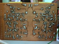
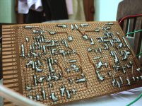
You are to be congratulated, in addition, for demonstrating that your breadboard layout dosen't oscillate, giving us normal hackers confidence to go at it!
This is just about what I wanted to see! Only 2 days ago I learned that MCM (in US) can source the laterals used here for a good price.
The Emitter deg is a nice touch (comes from a reader of Self!), and the low power is correct, esp with my having a nice 19-19V toroid around to use. I even have slews of 3.3v zeners!
Routinely I check power going into my usual listening setup, and get only 600mW or so, using the peak-hold setting on my multi. John Lindsey-hood was known for saying 1.5 watts is a reasonable level. (Mild-mannered Brit syndrome, perhaps) Bass, we know, is not there for the purpose of toasting nice 18 cm drivers, but for shunting to elemental drivers run by uncritical amps of primitive design, such as compl./symm. types running ancient to-3's, or even darlingtons!
You are to be congratulated, in addition, for demonstrating that your breadboard layout dosen't oscillate, giving us normal hackers confidence to go at it!
...Also, it should be noted that the low power supply voltage quite severely limits output power, by limiting the available current into the load because of limited maximum Vgs you can get. Laterals are particularly problematic here due to low transconductance, so lots of Vgs is required to turn them fully on. In theory, you could get the full 7A through the MOSFET with an output voltage of less than 10V peak, and that's assuming no supply voltage drop as current increases. Unfortunately, this is generally a problem with MOSFETs and low supply rails.
This is the case with any mosfet used as source follower. Although vertical fets have much more Gm and the change in Vgs vs Id is much less, it being exponential instead of square, Vgs threshold is almost 4V. Without a second higher voltage source for the VAS and drivers, it is not possible to drive the gate beyond the drain limiting rail to rail operation. BTW, In my last fet amp I bootstraped the driver stage.
") Clamping Vgs to limit Id would not provide short circuit protection, and after Id limit is reached, the driver stage would see the load in series with the gate stopper resistor. Eventually somthing would probably burn if continuously shorted. However I thought the intention was a simple way to temporarily limit Id peak into the load, and to learn how the transistors work before you blow them all up.
Clamping Vgs to limit Id would not provide short circuit protection, and after Id limit is reached, the driver stage would see the load in series with the gate stopper resistor. Eventually somthing would probably burn if continuously shorted. However I thought the intention was a simple way to temporarily limit Id peak into the load, and to learn how the transistors work before you blow them all up.
I cringe when I see mosfets wired to a PCB with long skinny wires. Mosfets make very effective oscillators. The verticals perhaps worse, but the resonance between the internal capacitances and lead inductances (including wires and PCB traces) can tank at very high frequencies (MHz) and require some sort of dampening, such as a gate stopper resistor. If an oscillation starts, Vgs limit to Id before the gate stopper may not save them from meltdown. Placing them onto the PCB will help.
Assuming you have an O-scope if you want to achieve maximum speed and lowest phase margin from the output transistors, on the PCB you can make two seperate ground tracks to your star and connect ~100R in series with 47pf from each gate to GND, right at the device pin. Then you can play with reducing the gate stopper resistor value. Start reducing it until you see a small burst of HF oscillation at the peak of the signal, then go back. Then you can play with the placement of the filter zero by adjusting the 100R resistor. Building a mosfet amp is not hard, maximizing it's capabilities....well thats the fun part.
This is just about what I wanted to see! Only 2 days ago I learned that MCM (in US) can source the laterals used here for a good price.
The Emitter deg is a nice touch (comes from a reader of Self!), and the low power is correct, esp with my having a nice 19-19V toroid around to use. I even have slews of 3.3v zeners!
Routinely I check power going into my usual listening setup, and get only 600mW or so, using the peak-hold setting on my multi. John Lindsey-hood was known for saying 1.5 watts is a reasonable level. (Mild-mannered Brit syndrome, perhaps) Bass, we know, is not there for the purpose of toasting nice 18 cm drivers, but for shunting to elemental drivers run by uncritical amps of primitive design, such as compl./symm. types running ancient to-3's, or even darlingtons!
You are to be congratulated, in addition, for demonstrating that your breadboard layout dosen't oscillate, giving us normal hackers confidence to go at it!
Thanks for your kind words colwaiting. The following picture is dedicated to nice guys like you! I know you can do it a lot better than me though.
All the best for your version of Magic.Have a nice day.
Attachments
The cap is there to 'overwhelm' the nonlinearity of the input capacitances of the MOSFET, so it should be about 10x worst case (Ciss || Crss) x 2 (x2 because of two MOSFETs in a pair). For a very small value of the trimmer, and correspondingly large value of the current in the driving stage, you can completely omit it as the trimer itself will have a low enough impedance to shunt the input capacitances.
I should mention that some different topologies for driving MOSFETs must NOT have this capacitor. In these, the MOSFETs are never turned off. However, in a simple amp like this, turning one MOSFET on fully requires Vgs of nearly 10V, while the Vgs required for ~100mA standing current is around 1V. This means that while one MOSFET is turned on fully, and has Vgs 10V, the other has -8V and is in a deep off state. If one looks at the Vgs/Vds versus Ciss/Crss curves, it becomes apparent that the P and N MOSFET are somewhat different so just charging and discharging these capacitances with the same constant current produces a crossover notch because of the difference in the Ciss curves. The notch itself happens with a 'delay' which depends on the charge/discharge current. Because of this 'delay' characteristic, the notch appears on different places in a waveform depending on frequency and amplitude, so you get a nonlinear form of distortion. The cap across the bias setting element (be that a trimmer or a transistor etc...) acts as a local 'buffer' so that much more current is available to circulate between the gates, essentially making both MOSFET gates look like one less complex capacitance to the driver, by 'buffering' the above discontinuity in Ciss. In theory, you could make it 'infinite' but in practise there are problems with frequency response of very large caps. A HF non-inductive cap is the right choice here, 10nF-1uF range.
IT should be noted that the discontinuity of Ciss between P and N CH types is still visible regardless of the capacitor due to the gate stoppers, because they limit charge/discharge current. Unfortunately, there is little that can be done against that, as the stoppers are a necessity. On the other hand, there is a different approach, where the crossover notch is 'modified' by the careful choice of gate stopper values. National Semiconductor has a very nice write-up about this in the documentation of one of their LMExxxx amplifier chips, as these use external power semiconductors (including MOSFETs).
Nice Ideas here Shaan - and project, of course. There's been some good input for problems many Mosfet builders have. Thanks guys.
Ilimzn, do you have a link or reference to that NS IC documentation you referred to back in post #7?
Thanks Ian.
I was also searching for it and found this. It is for LM4702 driver ICs. Still, it has a LOT of information on how to get the best of MOSFET power stages. Used FET families include 2SK(Renesas),2SK(Toshiba), BUZ(Magnatec) and(!) IRFP240/9240(IR). Is this the exact document that ilimzn mentioned in post 7? I don't know though.
http://www.national.com/an/AN/AN-1645.pdf
...
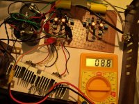
One thing I completely forgot to post is the output offset voltage.
Attached picture shows the offset which is +8.8mV for the current channel. The other channel showed -6.8mV when connected. Both of these are without any optimization, with default quiescent current of ~88mA and an 8ohm speaker connected. Disconnecting the speakers doesn't alter the offset. However, I have seen that at power up the offset rises to above 50mV for half a second and then quickly stabilizes to less than 10mV. The same happense at power down and is common in both channels. But nothing is heard of seen or felt on the speaker(cone moving or so...).
I suspect the charging delay of the feedback capacitor for this.
(the number 8 dominates... do you notice?)
Attached picture shows the offset which is +8.8mV for the current channel. The other channel showed -6.8mV when connected. Both of these are without any optimization, with default quiescent current of ~88mA and an 8ohm speaker connected. Disconnecting the speakers doesn't alter the offset. However, I have seen that at power up the offset rises to above 50mV for half a second and then quickly stabilizes to less than 10mV. The same happense at power down and is common in both channels. But nothing is heard of seen or felt on the speaker(cone moving or so...).
I suspect the charging delay of the feedback capacitor for this.
(the number 8 dominates... do you notice?
)Attachments
Last edited:
Well, I thought the LMExxxx was wrong but look what DIYaudio has in the Chip amp forum.I was also searching for it and found this. It is for LM4702 driver ICs. Still, it has a LOT of information on how to get the best of MOSFET power stages. Used FET families include 2SK(Renesas),2SK(Toshiba), BUZ(Magnatec) and(!) IRFP240/9240(IR). Is this the exact document that ilimzn mentioned in post 7? I don't know though.
http://www.national.com/an/AN/AN-1645.pdf ...
http://www.diyaudio.com/forums/chip-amps/102973-lme49810-new-cousin-lm4702-68.html. I assume this is it because the content seems right.
Thanks for the clue.
- Status
- This old topic is closed. If you want to reopen this topic, contact a moderator using the "Report Post" button.
- Home
- Amplifiers
- Solid State
- Magic - My first Lateral MOSFET Push-Pull amplifier