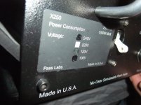
Marking on Back Plate for 220VAC but according the colored Leads 240VAC
What happened here ? The cables from primary winding were not re-soldered afterwards - otherwise one would see it at the soldering joints.
I didn't know that beforehand and therefore I soldered undesirably from 240V to 220V. In this configuration the power amplifier could not be switched on - maybe because too high inrush current. Therefore I remake the previous configuration for 240VAC according to the attached image.
I only took into account the marking on the rear of the panel but didn't take into account the color definition on the sticker of the transformer.
Attachments
Last edited:
Attachments
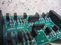
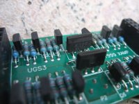
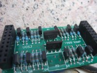
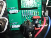
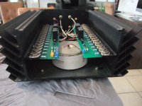
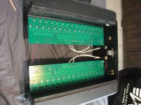
Follow questions rises up while looking the attached images (except the last three):
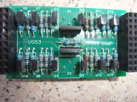
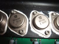
1) Why IRF 244 and not IRF240 as complement to the IRF9240 ?
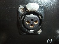
2) How to change the XLR plug (please note: this is a PCB version, mounted from outside, and not a version for manual wiring ?
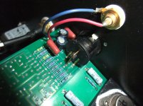
3) Why 100uF polarized electrolytics in the signal pad (neg. pole in direction to the XLR input pins) ?
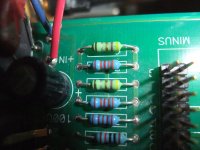
4) NFB capacitors in 4R7 resistor outline (maybe 4p7); what kind of capacitor is this ?
1) Why IRF 244 and not IRF240 as complement to the IRF9240 ?
2) How to change the XLR plug (please note: this is a PCB version, mounted from outside, and not a version for manual wiring ?
3) Why 100uF polarized electrolytics in the signal pad (neg. pole in direction to the XLR input pins) ?
4) NFB capacitors in 4R7 resistor outline (maybe 4p7); what kind of capacitor is this ?
Attachments
-
 DSCF6570.jpg1,000.7 KB · Views: 431
 -
 DSCF6571.jpg1,003.2 KB · Views: 389
 -
 DSCF6627.jpg999 KB · Views: 327
 -
 DSCF6615.jpg987.2 KB · Views: 383
 -
 DSCF6573.jpg998 KB · Views: 361
 -
 DSCF6572.jpg985 KB · Views: 367
 -
 DSCF6578.jpg1,000.3 KB · Views: 410
 -
 DSCF6588.jpg1,001.5 KB · Views: 423
 -
 DSCF6630.jpg1 MB · Views: 474
Last edited:
What happened here ? The cables from primary winding were not re-soldered afterwards - otherwise one would see it at the soldering joints.
I didn't know that beforehand and therefore I soldered undesirably from 240V to 220V. In this configuration the power amplifier could not be switched on - maybe because too high inrush current. Therefore I remake the previous configuration for 240VAC according to the attached image.
I only took into account the marking on the rear of the panel but didn't take into account the color definition on the sticker of the transformer.
Is it possible for the difference between 220VAC and 240VAC they make the adjustment with selecting different secondary taps.
I am guessing they only make the adjustment on the primary side when going from 220/240 down to 110/120.
I am not certain for that amp, but I do know many Pass Labs amps have transformers with multiple secondary taps for making adjustments.
Follow questions rises up while looking the attached images (except the last three):
1) Why IRF 244 and not IRF240 as complement to the IRF9240 ?
2) How to change the XLR plug (please note: this is a PCB version, mounted from outside, and not a version for manual wiring ?
3) Why 100uF polarized electrolytics in the signal pad (neg. pole in direction to the XLR input pins) ?
4) NFB capacitors in 4R7 resistor outline (maybe 4p7); what kind of capacitor is this ?
1) They most likely decided the transconductance of IRF244 was a more desirable match to IRF9240 for what they wanted.
2) If the XLR plug needs replacing, I am assuming it can be tossed in the bin, in which case I would use side cutters and cut the pins, then desolder the board using solder wick.
Last edited:
The XLR has a small hole for a straight screw driver so it comes out of the shell. Neutrik makes one but a jewelers type works.
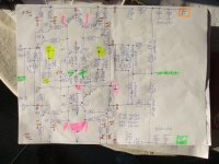
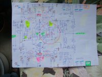
First Blueprint of UGS schematic
Intersil 283511, DS datasheet pdf
http://www.irf.com/product-info/datasheets/data/irf240.pdf
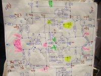
The schematic from the UGS module (own creating according the UGS board) is still riddled with many errors and incompleteness.
Especially the areas marked in red are incomplete or incorrect in my drawing.
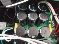
Next week or week after next the electrolytic capacitors with correct sizes have arrived.
Then I have another opportunity to take a closer look at the UGS board to correct or complete the circuit diagram.
The variable resistor in the neg. half must be arranged quite differently, because one is for the offset between the speaker outputs and the other for the offset between GND and "+ out" resp. GND and "- out".
But one thing can already be said currently: The operation in parallel mode of a MOSFET and a BjT in the VAS stage is not a sign of error. The question is, what is measured on the unused PINs 2 + 3 or 9 + 8? Just the voltage drop across the 6K8 resistor resp. the idle current of this stage?
P.S.: The MOSFETs on the left side of the drawing are not shown and the MOSFET for the quiescent current adjust is incorrectly shown (D + S swapped).
The caps are 4.7 pF ceramics. That is a pretty early unit But the transistors are correct.
The XLR has a small hole for a straight screw driver so it comes out of the shell. Neutrik makes one but a jewelers type works.
Good advices - thank you.1) They most likely decided the transconductance of IRF244 was a more desirable match to IRF9240 for what they wanted.
2) If the XLR plug needs replacing, I am assuming it can be tossed in the bin, in which case I would use side cutters and cut the pins, then desolder the board using solder wick.
Intersil 283511, DS datasheet pdf
http://www.irf.com/product-info/datasheets/data/irf240.pdf
The schematic from the UGS module (own creating according the UGS board) is still riddled with many errors and incompleteness.
Especially the areas marked in red are incomplete or incorrect in my drawing.
Next week or week after next the electrolytic capacitors with correct sizes have arrived.
Then I have another opportunity to take a closer look at the UGS board to correct or complete the circuit diagram.
The variable resistor in the neg. half must be arranged quite differently, because one is for the offset between the speaker outputs and the other for the offset between GND and "+ out" resp. GND and "- out".
But one thing can already be said currently: The operation in parallel mode of a MOSFET and a BjT in the VAS stage is not a sign of error. The question is, what is measured on the unused PINs 2 + 3 or 9 + 8? Just the voltage drop across the 6K8 resistor resp. the idle current of this stage?
P.S.: The MOSFETs on the left side of the drawing are not shown and the MOSFET for the quiescent current adjust is incorrectly shown (D + S swapped).
Attachments
Last edited:
If you send a PM to Zen Mod he can probably give you lots of good tips regarding servicing your amp.
It's possible there might be upgrades for this topology in later revisions of the amp.
If you're going to the effort of replacing components it might be worthwhile knowing if there are any recommended changes/improvements while you're working on it.
It's possible there might be upgrades for this topology in later revisions of the amp.
If you're going to the effort of replacing components it might be worthwhile knowing if there are any recommended changes/improvements while you're working on it.
Yes, this is only possible on the primary side - go to images 6-9 from sticker of transformer in post #19.Is it possible for the difference between 220VAC and 240VAC they make the adjustment with selecting different secondary taps.
I am guessing they only make the adjustment on the primary side when going from 220/240 down to 110/120.
I am not certain for that amp, but I do know many Pass Labs amps have transformers with multiple secondary taps for making adjustments.
Regardless, it is strange that the labeling on the back plate and the actual setting of the colored transformer cables are different.
Last edited:
How does amps like these sound if connected to speakers where an amp like ACA is more than enough power?

I think it could be personal.
Some people love the sound of 2nd harmonic in generous quantities others prefer a very neutral sound.
On the positive side with an amp like this you could always add a tube preamp, if that was your preference.
On speakers such as what you are suggesting an XA30 is more than enough.
Some people love the sound of 2nd harmonic in generous quantities others prefer a very neutral sound.
On the positive side with an amp like this you could always add a tube preamp, if that was your preference.
On speakers such as what you are suggesting an XA30 is more than enough.
They may be good for Magneplan speakers which I think go low in impedance.......and they are not very efficient either.....
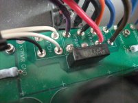
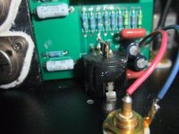
A closer look to the primary winding of the transformer confused me a little.What happened here ? The cables from primary winding were not re-soldered afterwards - otherwise one would see it at the soldering joints.
I didn't know that beforehand and therefore I soldered undesirably from 240V to 220V. In this configuration the power amplifier could not be switched on - maybe because too high inrush current. Therefore I remake the previous configuration for 240VAC according to the attached image.
I only took into account the marking on the rear of the panel but didn't take into account the color definition on the sticker of the transformer.
According to the sticker on the transformer the colors orange-blue-violet (post #19, page 2, image 6-8) stands for 0-100-120VAC
According to the soldering performed (go to second image in post #21, page 3) the colors violet-blue-orange stands for 0-100-120VAC
What is correct and what is wrong?
To find out this I use a standard tubular halogen lamp in series to the primary winding of this transformer.
Here the datasheet of these lamp:
https://docs.rs-online.com/ac69/0900766b812827fa.pdf
and of the light housing:
Halogen Light H 500 IP54 400W 8545lm black | brennenstuhl(R)
In the right configuration the brightness is very high immediately after switch on, but the light goes out within 1-2 seconds after switch on. In the wrong configuration the brightness remains, because then the inductance of both primary windings cancel each other out to zero.
The soldering performed according second image in post #21 provided the correct result and the sticker of transformer clearly shows a misprint here, because orange and violet were swapped when executing the lettering.
BTW - Such a lamp helps to find out the right answer in similar situations and is a very interesting replacement for a usual ceramic 10-W resistor in a inrush current limiter.
.
Good advices - thank you.
Intersil 283511, DS datasheet pdf
http://www.irf.com/product-info/datasheets/data/irf240.pdf
The schematic from the UGS module (own creating according the UGS board) is still riddled with many errors and incompleteness.
Especially the areas marked in red are incomplete or incorrect in my drawing.
Next week or week after next the electrolytic capacitors with correct sizes have arrived.
Then I have another opportunity to take a closer look at the UGS board to correct or complete the circuit diagram.
The variable resistor in the neg. half must be arranged quite differently, because one is for the offset between the speaker outputs and the other for the offset between GND and "+ out" resp. GND and "- out".
But one thing can already be said currently: The operation in parallel mode of a MOSFET and a BjT in the VAS stage is not a sign of error. The question is, what is measured on the unused PINs 2 + 3 or 9 + 8? Just the voltage drop across the 6K8 resistor resp. the idle current of this stage?
P.S.: The MOSFETs on the left side of the drawing are not shown and the MOSFET for the quiescent current adjust is incorrectly shown (D + S swapped).
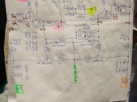
New caps arrived last weekend and most of the errors in this circuit diagram should now be eliminated.
Now the follow questions rises up:
1) The source pins of 2SK389 (upper dual j-FET from positive half) use a common resistor, but not the 2SJ109 (lower dual j-FET from neg. half). What special properties do one get?
2) P1 (positive half) is used to set the offset from the speaker outputs to GND.
Unfortunately, even a minimal change in the setting results in large voltage differences (in opposite to P2 in the neg. half).
What can one do to achieve the same change behavior as on P2?
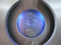
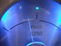
3) According some images of the ampere meter at the front on the web I adjust the idle current for output buffer. Result: 110-120mA each MOSFET (55-60mV each resistor) corresponds 1,85mA for each channel at whole. Is this the right value (thereby arise a temperature of 20-22°C above ambient) ?
4) Idle current of UGS-modul amounts 20mA at right channel and 24mA at left channel (1,22 VDC at one channel and 1,07VDC at the other channel - measured voltage at 47R/3W). Is this in the allowed area ? And what is the value for voltage drop across the 6K8 resistors to Q7/8/9/10/11/12/13/14 and 10K to the drains of Q1/2 ?
5) What happens, when I connect an unbalanced preamp driver stage (I observe an audible hum at both channels) ?
Maybe, because one pin of both from balanced input isn't connect ? Then an input transformer like a Lundahl LL1592 - go to
https://www.don-audio.com/mediafiles//datasheets/1592.pdf
is necessary.
Thank you for all wanted information.
Attachments

Last edited:
1. there is a proper common resistor between JFets sources, you're just confused with so called McMilan resistors, going to outputs; no need to break common nresistor in two and connect McMilan's to mid point
2. break trimpot value in two fixed resistors - left and right, and smaller trimpot value; Boyz and Girlz in PL are evidently having finer hands than Greedy Boyz have
3.set amp Iq to desired value, then just set needle in mid position, in temp. equilibrium
4. Iq of UGS is good; rest is self explanatory
5. PL is delivering amp with U shortie, put in 1&3 XLR pin holes ; that's your trick for SE input
btw. plenty of applicable tricks you can find here, even if there is no schm : Pass Labs X150.5 , checking/adjusting offsets ,Iq and gain - Zen Mod Blog
Bugs in the feedback networks ?
- If your drawing is right, IMO the 68Ohms is solely implemented to reduce transimpedance of the input stage AND (!!) to avoid that one of the pairs (most likely the SJ109) goes into "positive" Vgs, which means leakage currents and non linearity
- I think you have a bug in the feedback networks ! Please see appended markups in your schematics, which make much more sense to me.
This is also supported by Nelson Pass' post in the following thread:
Aleph-X builder's thread.
Post #1655
By using a 120R to ground at summing junction, the open loop (noise-) gain is reduced to about 69dB. This would be still at the level of a good OPA at 20kHz and it would also explain the high sensitivity of the circuit to pot changes.
- The use of 10kOhms as "gate stoppers" is extremely strange.
- Are you sure, that there is capacitive coupling in the inputs ??? I think this is against all marketing claims of Pass Labs.
Attachments
- Home
- Amplifiers
- Pass Labs
- Pass X250 repair