PL never said anything against capacitive coupling
not sure and lazy to check, but I believe there were not claims of DC coupling
not sure and lazy to check, but I believe there were not claims of DC coupling
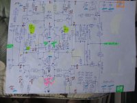
Thanks for all hints. The electrolytic capacitors in the signal pad together with bypass of 0,47µF are definitely present without the possibility of optional shorting for using as DC coupled input.- If your drawing is right, IMO the 68Ohms is solely implemented to reduce transimpedance of the input stage AND (!!) to avoid that one of the pairs (most likely the SJ109) goes into "positive" Vgs, which means leakage currents and non linearity
- I think you have a bug in the feedback networks ! Please see appended markups in your schematics, which make much more sense to me.
This is also supported by Nelson Pass' post in the following thread:
Aleph-X builder's thread.
Post #1655
By using a 120R to ground at summing junction, the open loop (noise-) gain is reduced to about 69dB. This would be still at the level of a good OPA at 20kHz and it would also explain the high sensitivity of the circuit to pot changes.
- The use of 10kOhms as "gate stoppers" is extremely strange.
- Are you sure, that there is capacitive coupling in the inputs ??? I think this is against all marketing claims of Pass Labs.
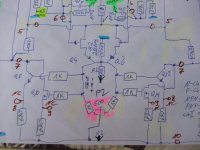
The 10k resistors should actually all be measured because the colors orange, red and brown - which define the number of zeros - all
look almost identical, i. e. the resistors could have a value of 1K, 10K and 100K. This I will do while next session for faultfinding.
Either the NFB network is wrong in my own created schematic or the outputs [C, Q3(4) and C, Q5(6)] are swapped.
So the question is whether each half operates in the inverted or non inverted mode.
Also this I will check again.
Last edited:
These were cap coupled on the inputs. The .8 series are not but maybe should be given some of the products they connect to.
Except the 10K resistors R1,2 for Uref all showed 10K resistors have only 1K. Additional all showed 6K8 resistors have 680 ohms.Thanks for all hints. The electrolytic capacitors in the signal pad together with bypass of 0,47µF are definitely present without the possibility of optional shorting for using as DC coupled input.
The 10k resistors should actually all be measured because the colors orange, red and brown - which define the number of zeros - all
look almost identical, i. e. the resistors could have a value of 1K, 10K and 100K. This I will do while next session for faultfinding.
Either the NFB network is wrong in my own created schematic or the outputs [C, Q3(4) and C, Q5(6)] are swapped.
So the question is whether each half operates in the inverted or non inverted mode.
Also this I will check again.
the showed 120 ohm NFB resistor have 10K and the showed 12K2 resistor have 22K and must connected from GND to the node 332K/10K and disconnected from the node 10K/100uF| | 0,47uF.
Each half operates in the inverted mode, i.e. the pos. output goes about 332K to the gate of left half from Q1/2 and the neg output to the gate of right half from Q1/2. Thus this wasn't an error by drawing.
Last edited:
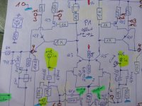
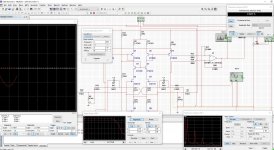
last update of my schematic - attached supplement to my previous post.
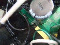
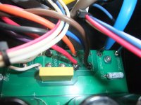
After removing the doubly present capacitors between the 230VAC manis connections and the chassis no audible hum is present.
Two capacitors was on the supply PCB (fifth and sixth image) and two in the integrated filter of mains input plug (seventh image, replace by an input plug without integrated parts).
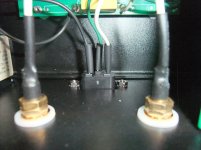
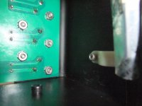
Last both images show the clamp resp. clip for fixing the thermal fuse. But it is impossible to do this.
The final step requires obtaining a good quality clamping fixture as well as drilling new holes in the heat sink (disassemble again is necessary unfortunately).
I'm not really enthusiastic - a detailed report of all deficiencies will follow together with the residual circuit diagrams.
After removing the doubly present capacitors between the 230VAC manis connections and the chassis no audible hum is present.
Two capacitors was on the supply PCB (fifth and sixth image) and two in the integrated filter of mains input plug (seventh image, replace by an input plug without integrated parts).
Last both images show the clamp resp. clip for fixing the thermal fuse. But it is impossible to do this.
The final step requires obtaining a good quality clamping fixture as well as drilling new holes in the heat sink (disassemble again is necessary unfortunately).
I'm not really enthusiastic - a detailed report of all deficiencies will follow together with the residual circuit diagrams.
Attachments
-
 UGS- Modul + Buffer SN11651 last update-I.jpg838 KB · Views: 982
 -
 UGS- Modul + Buffer SN11651 last update-II.jpg760.1 KB · Views: 958
 -
 UGS- Modul + Buffer SN11651 last update-III.jpg799.1 KB · Views: 1,227
 -
 UGS- Modul + Buffer SN11651 last update-IV.jpg839.9 KB · Views: 855
 -
 DSCF6663.jpg996.1 KB · Views: 769
 -
 DSCF6638.jpg982.2 KB · Views: 499
 -
 DSCF6662.jpg1,012.5 KB · Views: 414
 -
 DSCF6656.jpg1,005.2 KB · Views: 463
 -
 DSCF6655.jpg995 KB · Views: 622
Last edited:
according the instruction manual resp. owner's manual the circuit topology from x250 is according those from SuSy patent - go to
PassDiy
i. e. designed as folded cascode and thus a single gain differential amplifier stage (that means lower open loop gain).
according my own created schematic from X250 the circuit topology consist of a differential amp as input stage and a voltage amplifier stage (VAS) as driver for the following source follower. This topology is very similar and more close to that of the simplified schematic from first image in the attachment than that of the SuSy patent
This simplifiied schematic from INT-150 I have found under
Pass SuSy Verstarker haben doppelten Differenzverstarker am Eingang - Visaton Diskussionsforum
i. e. designed not as folded cascode and thus two voltage gain stages (that means higher open loop gain).
This image was published in German's magazine "Stereoplay" from 2008 (second attached image is the cover), test report from INT-150, issue from july.
Why isn't mentioned this fact in the owner's manual of X250 ?
Which of the power amplifiers from the X-XA-XS series actually have a single-gain stage according to the patent (folded cascode) and which do not like X250 ?
Attachments

Last edited:
I don't treat cascodes or constant current sources as gain stages. To me, a
cascoded transistor represents a single stage.
cascoded transistor represents a single stage.
OK, contrary to things presented in patent itself (No. 5376899, "Amplifier with gain stages coupled for differential error correction" , easier to get through PAT2PDF - Free PDF copies of patents: Download and print! )** - I can't remember any example of PL X amp having folded cascode FE
as far as I know - all were equipped with UGS stage ( several gen.), with one or few exceptions (X350 yes, any other? lazy to rummage more through plethora of folders), and even then there wasn't folded cascode anywhere .......
so, almost all covered with explanation of 2 stages ( per phase ) : when looking at FE as whole , UGS is inner ring, outer ring made of common source arranged mosfets, each ring representing one stage of amplification
after that less or more funny biasing stage , then PP source follower OS , which I'm usually representing mentally as 4 quadrants arrangement, as 3rd ring in entire shebang
**maybe I dreamed about ( often having wild dreams, including extremely comic ones), but I think I read or heard Pa saying that in time of patenting bloody thing, he didn't comprehend half of things he learned later, using SUSY for later work; anyway, in entire story, folded cascodes or not, pretty irrelevant detail....... I'm sorta jus semi splitting da hair here, in name of establishing some historical facts, nothing more
btw. our Frenchy guys made very functional SUSY amp iteration (Up Amp), using current mirrors as way of modulation of outer ring of that UGS module ....... further ....... it can be made with folded cascodes, but then one must count on additional problems - necessary increase in rails voltage etc. .... pretty much dubious benefits, counting how efficient and elegant basic UGS is, both in performance and function
and, do not we forget - Wayne gave us (for free!!) UberFunnyGenial simple UGS - using just N channel JFets , in his BA2018 presented Line Stage
This posts don't provide for me comprehensible explanations.
But in the case of distortion behaviour from complementary differential jFET-pair vs. not complementary differential pair in the front-end this URLs are of interest:
F5X -- the EUVL Approach
the URL in this thread - go to
404 Not Found
is death.
currently valid URLs are here:
Distortion in JFET input stage circuits
or archived from 2011
Distortion in JFET input stage circuits
Last edited:
I did replied to your question:
As far as I know, none of the power amplifiers from the X-XA-XS series actually have a single-gain stage according to the patent (folded cascode)
As far as I know, none of the power amplifiers from the X-XA-XS series actually have a single-gain stage according to the patent (folded cascode)
I don't treat cascodes or constant current sources as gain stages. To me, a
cascoded transistor represents a single stage.
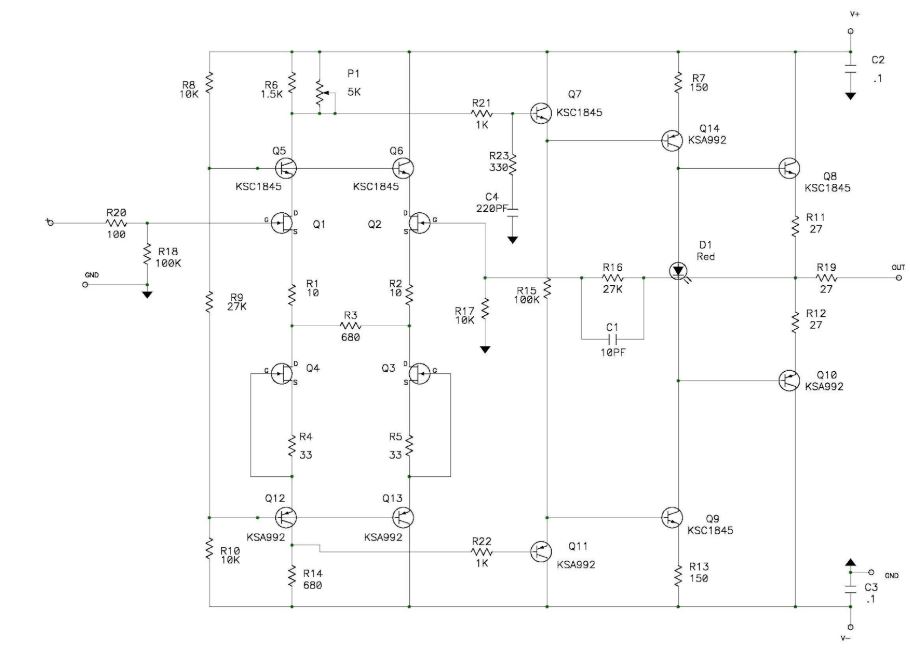
For me the reverse engineered X-250/UGS3 circuit contains THREE STAGES:
1) The input pairs
2) The VAS (actually current mirrors, NO its not a folded CASCODE)
3) The power output stages
From my own experiences with designing PA amps in the 90ies, driving a bank of eight IRF MOSFETs by simple current mirrors is a MAJOR DESIGN FLAW. I can only recommend to introduce drivers for the power stage.
Even SuSy doesnt help here a lot.
Last edited:
From the official X-250 broschure:
The amplifier uses ultra-matched components in a simple balanced Class A circuit. It contains only two gain stages. A balanced single-ended Class A voltage stage drives a bank of large wattage/high power metal can Mosfets operated as followers with a minimal amount of feedback around the output stage. The X250 accepts single-ended inputs via RCA connector and balanced inputs via XLR connector.
The SuSy patent with its folded cascode two stage architecture is always cited in PassLabs literature (press texts, user manual, bruschures) for this series.
The two stage "simple" architecture is a plain legend.
two stages of voltage gain, OS is follower
SUSY yes, but who cares about folded cascode - it is irrelevant detail
boys, your'e splitting da hair here, get a life
edit - and there are no current mirrors in X250, nor in any UGS module gen. , that I'm aware of
SUSY yes, but who cares about folded cascode - it is irrelevant detail
boys, your'e splitting da hair here, get a life
edit - and there are no current mirrors in X250, nor in any UGS module gen. , that I'm aware of
Last edited:
The reason I got upset here is, that NP has the balls to defend the dishonest marketing blah, his company is spreading now for more than two decades. This really doesn't fit his stellar rep.
If I read tiefbassuebertr's reverse engineered schematics right,
the X-250 amplifier is NOT:
- A two stage design like suggested in his literature/patent
- A DC coupled design
- A design with a mind blowing 148dB dynamic range by any accepted measurement standard
Anyhow all of that can be read out of PassLabs literature...
Please give me the "real" circuit, which shows that X-250/UGS3 doesn't contain a current mirror and/or VAS or coupling capacitors and a measurement which shows these dramatic 148dB.
Tiefbassuebertr's had some easy to answer questions and only got foggy responses and I'm pretty sure, what the reason is !
Last edited:
-two gain stages
-show false claims; read this : https://www.passlabs.com/wp-content/uploads/2020/05/x250_om.pdf
-can't say anything for 150db dynamic range, but I'm having much lesser computational ability than Pa, and obviously much lesser than you
........ I have X250/UGS service manuals and schematics, and there is no Current Mirror
Tiefbass got most of answers, now - who's eager to read them and understand, that's other question
and - btw. reading and believing too much in FiFI periodicals isn't good neither for brain nor for morale; though, when one is just looking at pictures, there can be some benefits for gray matter
Indeed, for most buyers today, this is how you put it (probably for everyone in 5-10 years).two stages of voltage gain, OS is follower
SUSY yes, but who cares about folded cascode - it is irrelevant detail
boys, your'e splitting da hair here, get a life
But for people for whom it is both important to acquire the best possible sonic quality and who want to know why that is so, this is a very important detail in the circuit.
These differences also exist in the circuit design of operational amplifiers and, as a result, different focus areas arise;
this is a typical one gain stage architecture - go to page 10 under
https://www.analog.com/media/en/technical-documentation/data-sheets/AD817.pdf
this is a typical two gain stage architecture - go to page 8 under
https://www.analog.com/media/en/technical-documentation/data-sheets/AD744.pdf
and page 2/15 under
https://www.st.com/resource/en/datasheet/tl081.pdf
I now understand very well why circuit diagrams resp. schematics and service manuals are not published on a large scale (by almost all companies).
Otherwise, many manufacturers would be bombarded with questions in the same way as I asked them - resulting from the actual kind of operation and circuit description mentioned in the associated patents, brochures and owner's-/ instruction manuals deviate from it to a greater or lesser extent.
Another example of poetry and truth (from countless others) is Carlos Candeias approach "LEF" - check out post #10 under
https://www.diyaudio.com/forums/pass-labs/5808-cec-amp71.html#post3435797
and his own explanation under
http://www.hifi-weiler.de/fileadmin/media/LEF-Technik.pdf
and this URL's:
LEF (Load Effect Free) Amplifier technology
C.E.C AMP3300R (3300 R Amp 3300R Amp3300) and AMP5300R LEF Class A schematic wanted
BTW: sound is at least of the CEC model Amp-3300 and B.M.C. model "C1" hard and crispy and absolutely unsatisfactory.
Evidence of that is here:
https://www.stereophile.com/content/bmc-audio-amplifier-c1-integrated-amplifier-measurements
go to Fig. 9 and 10.
If the corresponding schematic was known for me, I would not even have unpacked and connected that devices for a listening test.
In the meantime, however, I don't care more and more because the real interest in high-quality sound reproduction is waning more and more.
Unlike in the past, it is extremely important today that users only believe they have the best audio devices (whether this is actually the case is now mostly unimportant) - the prerequisite for this is perfect optical outline for most residential environments (today even the eye listens), perfect advertising/representation/marketing and excellent test reports without the slightest criticism.
Last edited:
........
In the meantime, however, I don't care more and more because the real interest in high-quality sound reproduction is waning more and more.........
well, don't be hypocritical ....... if anyone, Papa with his activities here is in fact doing something for us Greedy Boyz - showing to all of us what is his way of making High Fun (call it High End, if you wish) ...... besides all complete projects for FW and pre-FW amps, he gave more than enough info about PL Products
anyway, enough from me - if someone made situation for arguments and insist of it, mine is to give some arguments ( in best intentions - to share what I know, not to be one who is right) and when those arguments are not heard, why should I care further
bye
The schematic from PDF in post #7 underI did replied to your question:
As far as I know, none of the power amplifiers from the X-XA-XS series actually have a single-gain stage according to the patent (folded cascode)
Pass X250 concept ?
looks interesting, because it is much more close to those topology from SuSy patent.
When I replace the current mirrors (which serves as level shifters) by a folded cascode (of course with simultaneous change of the polarity from the signal inputs), then I will get the topology from patent with only a negligible difference:
Instead of a folded cascode I have a nesting of a normal and a folded cascode.
But definitely then there is only one voltage gain stage (according the patent) present.
Without having tried or tested it myself, I am sure that the replace of the UGS module by this circuit from post #7 provide better sonic results by a listening test, as long as no new errors nestle in the implementation.
BTW - the attached file from post #12 under
Pass X250 concept ?
shows also a schematic with two voltage gain stages, which is close to my own created schematic from X250, but
possibly with an improved offset setting (location of VR2 for offset between the outputs and GND could be crucial here).
Post #1339 under
UGS adventures
shows schematic file of the tested version with the current mirrors, which I will save here:
Attachments
Last edited:
Wow. You never know when old posts will come back to haunt you. In fact, that post taught me never to post a schematic without building and verifying a circuit first.
The circuit did get built after the errors were fixed. I removed the followers and added a couple of extra output transistors to each of the mirrors to hike up the output current. The resulting line amp sounded very detailed, clean and spacious. It lived in my system for several months until it was replaced by something else. It still sits on shelf in my garage. Maybe I’ll drag it out and have another listen.
I do miss Grey.
Graeme
Last edited:
I think when the output current of the mirror is significantly larger
than the input current you probably want to think of it as a gain stage.
The question of why one might switch to having a second stage in the
front end has a simple answer in my case - I wanted to use the Toshiba
2SK170 / 2SK74 Jfets for the inputs instead of the existing power Mosfet
parts. The folded cascode or current mirrors require current from the input
pairs as large as the output current which has to drive the capacitance of
the output stage.
10 mA bias simply didn't cut it, and I wasn't ready to parallel large
quantities of those parts. In hindsight, it was a good decision...
- Home
- Amplifiers
- Pass Labs
- Pass X250 repair