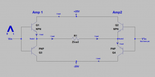
Class aP BTL Power amp
The asc file in the previous post shows the exact schematic I used to hardwire the prototype, and not the one shown next to the pic of the prototype. Please note that the outputs of the precision rectifier are depicted as positive going triangular pulses with a time duration under each. There is also an output +ve DC offset of <10 mV on them too. Each pulse starts at zero V, it peaks to a certain voltage, and then returns to zero V during its time interval.
The power amp was described in post #28. It is part of an Optimus STA-2160 receiver. Both power amp channels therein were used to generate the Bridge Tied Load format [BTL]. Both amps are DC coupled; meaning there is not an input coupling capacitor. I have two Optimus receivers to make a Right and Left stereo system. Please note the following additional changes that were made to the power amps of each Optimus receiver:
1. Each channel has a pot at the input diff amp to trim DC offset at its power output such that when the load is BTL-connectd, the net DC across it was <50 mV.
2. The power supply rails of the parent power amps are +/-60 Vdc. I separated their power output stages from this original status and gave them a +/- 25Vdc rails. The front end, and the VAS continued to be powered by the parent +/60Vdc.
3. I measured an idle bias of ~5 mA max in the BJT power output stage with the +/-25 V power rails. The bias regulator of each amp is not adjustable.
The left schematic is a simplified depiction of the power output stages [each idling at ~5 mA bias] of amps 1 and 2. Note the following operation due to the presentation of Vin triangle pulse to Amp 1 during the time interval of 0 to t. Amp 2 is idle because its input plulse has not arrived yet.
1. NPN of Amp1 conducts. Its output current flows out of its emitter [Node 1] through the load, and reaches Node 2.
2. At Node 2, PNP of Amp 2 conducts the load current, and routes it to the -25Vdc rail.
3. Node 2 is a virtual ground and is enforced by Amp2 which operates in the common base configuration; because load current enters the emitter of it PNP.
4. The conduction of PNP of Amp2 runs the real risk of exceeding its SOA; because its Vce is always locked at -Vee. This is the principal reason I lowered the parent -Vee from 60 V to 25 V after both of the original power PNPs blew because of a presumed SOA violation.
The right schematic is the same depicted BTL output stage; except V'in is presented to the input of Amp2 during the later time interval of t to t1 of the pulse. The input signal Vin to Amp 1 is already gone. Note that the load current flows from the emitter of NPN of Amp2 through the load, through PNP of Amp1 to -25V. Node 1 is now a virtual ground.
Some thoughts; say for the left schematic:
1. NPN of Amp1 and PNP of Amp2, simultaneously, and equally conduct load current. Both BJTs [NPN1, and PNP2] may be considered to pertain to one amp as a complementary pair.
2. By comparison, in a standard Class A amp, as its power NPN conducts more, its complementary power PNP conducts less.
3. By comparison, in a standard Class B amp, as its NPN conducts more, its PNP is off.
I've been using this system for a while. A CD source which is a volume controlled headphone output, drives the precision rectifier which drives the BTL amp. There is no hum or hiss in the loudspeakers. It sounds great, and maybe subjectively different from other amps; because of it type of operation.
Attachments

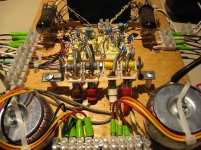
This is shown in the attached image. The circuit was assembled on a perf board, and enclosed in a Tuperware container which simplified drilling for the feed through of input, output and power lines. It shows a Right and a Left channels. The schematic which is attendant to each channel of the device is shown. Please note the following:
1. The first stage [rectifier] is LF356N instead of the LT opAmp which I used solely to run the simulation.
2. The output buffers are one dual OPA2134.
3. Chose switching diodes with the lowest forward voltage drop when passing 1 mA through. I chose 2 ~ matched diodes at 0.6 V.
4. Note the constant current sources [I1 and I2] using the 2N3819 JFETs to the left of the schematic. The resultant voltage drops of ~0.4 V across the 220 Ohm resistors forward biases the switching diodes for faster turn on.
5. The simulation runs smoothly as shown when using the attached asc file.
This precision rectifier may loosely be called an "analog source". It drove a power amp the output stage of which was configured as a Bridge Tied Load {BTL} which I'll elaborate on in a following post.
The OpAmp [LF356N] which I have used to date [point 1 above] is roughly a 40-year-old design. I recently replaced it with OPA134PA. It is a current state of the art design which is specifically geared for high fidelity audio. An improvement in the resulting subjective sonics was readily discernible. The music became relaxed. The high end was especially detailed and crystal clear.
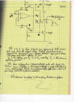
I was inspired by the diversity of schematics in Sounhappy's thread*****Goldmine of DIY audio tubes schematics from Japan*****. So I assembled a Class aP headphone amp based on 12AX7A. The application of Class aP to tube/valve amplifiers has been a pending objective. I hope to soon start a new thread in the Tubes/Valves forum to be entitled " Experimenting with Class aP Tube/Valve Amplifiers".
Please find attached a partial schematic of this 12AX7A headphone amp and a photo of its prototype. Sounds great.
The generator in use for the [analog Pulses] was shown in post#200.
This application to tubes/valves is a natural slam-dunk.
Best
Anton
Please find attached a partial schematic of this 12AX7A headphone amp and a photo of its prototype. Sounds great.
The generator in use for the [analog Pulses] was shown in post#200.
This application to tubes/valves is a natural slam-dunk.
Best
Anton
Attachments
Thanks ZM. I am also dreaming of EL84s in this app. soon.12AX7 is sissy , good for mV signals on grid
use something with more cojones , at least 6DJ8
A Class aP Headphone Amp
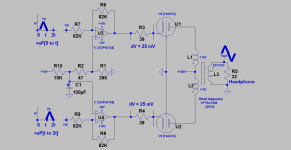
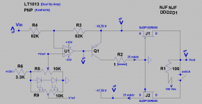
Commercial headphones have high sensitivity. They require a minuscule amount of power to drive them. The attached schematic is for a Class aP headphone amp. It is is essentially the generator of analog pulses which I already showed assembled in post#200. There is absolutely no need to complicate it further [for this app] by post-adding devices like buffers, vacuum tubes etc.
There is nonetheless a complication. The headphone plug must be cut so as separate the leads to each load [ear]. This is a Bridge-Tied-Load [BTL] like application. Both loads no longer share the common ground of the plug.
I am experimenting with a stereo headphone called Panasonic XBS which has lost both of the foam ear cushions. Each independent load is a 24 Ohms resistor. The scope showed positive-going music analog pulses of ~10 mV peak at each end of the load.
This stereo headphone/amp combo sounds fully satisfactory.
Best
Anton
Attachments
Making a two-channel Class aP power amp
The output stage of a Class A/B push-pull vacuum tube power amp requires its pair of tubes to be matched for gain as a function of frequency, plate current and etc. This narrative fully applies to a "like" Class aP push-pull power amp using SJDP120R085 [example] as a substitute solid state vacuum tube [pentode]. Device [tube or semiconductor] matching enables a high accuracy of amplification and thus less reliance on overall negative feedback.
Please note this important precedent. Dr. Michael S. Mazzola currently of iMPOWER Systems had successfully substituted 6L6 vacuum tubes with R085s in a Fender guitar amp. A picture of his new approach/amp is found in the thread "SemiSouth boiler room".
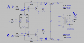
The attached schematic is a partial for a transformer-coupled power output stage of an actual Class aP amp using two SJDP120R085. Lots of detail to cover in this and following posts:
1. The two JFETs operate in the common gate configuration.
2. The JFETs were given to me by Mr. Pass while experimenting with DEF.
3. OpAmp U1 [1/2 OPA 2134 actual ] generates bias for J1 by installing a specific voltage [+6.76 V] at its source [+Vsg].
4. This +Vsg enables an idle ~25 mA to flow out of J1's source.
5. OpAmp U1 inverts the phase of Vin analog pulse. Thus it presents the source pin of J1 with a negative going analog pulse of voltage gain = 1.
6. The limited output current capability of U1 is augmented with Q1 power PNP which has an hfe of ~100.
7. PNP sinks the current [idle and due to analog pulses] from the source of J1 to ground.
8. The 1 Ohm sense resistor in the collector circuit of Q1 is to adjust the idle bias of J1. Protect this Unobtainium JFET from excessive power dissipation.
9. J2 [bottom R085] has an identical circuit [not shown] like J1. Meaning an OpAmp [U2, the second 1/2 of OPA2134], and a Q2 power PNP.
10. The circuit containing the two LEDs generates the [+Vrefs] to the 2 OpAmps. [+Vref] is amplified [X2] by OpAmp to become [+Vsg] for the destination JFET.
11. Each JFET needs its own [+Vsg] so to idle at 25 mA at a Vds of ~100 Vdc. The value of +Vsg for each JFET is encircled on the partial schematic.
12. Thus, I have two mirror image circuits for J1 and J2. Bias to each JFET is readily and independently adjusted so to enable ~identical drain/source currents. Idle conditions are ~stable; meaning minimum up-drift of the drain current of each JFET.
The mirror image circuits of J1 and J2 are matched for gain:
1. The drains of the JFETs are tied together; meaning a summing junction at [Vout]
2. Both JFETs have a common 100 Ohm load resistor which terminates to 105 Vdc.
3. Note the mechanical on/off switch in the drain circuit of J2. Keep it open
4. Apply the same analog pulse train to the inputs of both circuits. The same means a pulse which has the same active time duration denoted as [0 to t] or [t to t1]; meaning in-phase.
5. Measure Vout on the scope.
6. Close the mechanical switch in the drain circuit of J2. Measure the new Vout which is found to be double the value of that found in #5. Gain Match has been attained.
I'll show the full schematic of this R channel, and back fill added detail. It sounds pleasantly great, and without the use overall negative feedback.
The output stage of a Class A/B push-pull vacuum tube power amp requires its pair of tubes to be matched for gain as a function of frequency, plate current and etc. This narrative fully applies to a "like" Class aP push-pull power amp using SJDP120R085 [example] as a substitute solid state vacuum tube [pentode]. Device [tube or semiconductor] matching enables a high accuracy of amplification and thus less reliance on overall negative feedback.
Please note this important precedent. Dr. Michael S. Mazzola currently of iMPOWER Systems had successfully substituted 6L6 vacuum tubes with R085s in a Fender guitar amp. A picture of his new approach/amp is found in the thread "SemiSouth boiler room".
The attached schematic is a partial for a transformer-coupled power output stage of an actual Class aP amp using two SJDP120R085. Lots of detail to cover in this and following posts:
1. The two JFETs operate in the common gate configuration.
2. The JFETs were given to me by Mr. Pass while experimenting with DEF.
3. OpAmp U1 [1/2 OPA 2134 actual ] generates bias for J1 by installing a specific voltage [+6.76 V] at its source [+Vsg].
4. This +Vsg enables an idle ~25 mA to flow out of J1's source.
5. OpAmp U1 inverts the phase of Vin analog pulse. Thus it presents the source pin of J1 with a negative going analog pulse of voltage gain = 1.
6. The limited output current capability of U1 is augmented with Q1 power PNP which has an hfe of ~100.
7. PNP sinks the current [idle and due to analog pulses] from the source of J1 to ground.
8. The 1 Ohm sense resistor in the collector circuit of Q1 is to adjust the idle bias of J1. Protect this Unobtainium JFET from excessive power dissipation.
9. J2 [bottom R085] has an identical circuit [not shown] like J1. Meaning an OpAmp [U2, the second 1/2 of OPA2134], and a Q2 power PNP.
10. The circuit containing the two LEDs generates the [+Vrefs] to the 2 OpAmps. [+Vref] is amplified [X2] by OpAmp to become [+Vsg] for the destination JFET.
11. Each JFET needs its own [+Vsg] so to idle at 25 mA at a Vds of ~100 Vdc. The value of +Vsg for each JFET is encircled on the partial schematic.
12. Thus, I have two mirror image circuits for J1 and J2. Bias to each JFET is readily and independently adjusted so to enable ~identical drain/source currents. Idle conditions are ~stable; meaning minimum up-drift of the drain current of each JFET.
The mirror image circuits of J1 and J2 are matched for gain:
1. The drains of the JFETs are tied together; meaning a summing junction at [Vout]
2. Both JFETs have a common 100 Ohm load resistor which terminates to 105 Vdc.
3. Note the mechanical on/off switch in the drain circuit of J2. Keep it open
4. Apply the same analog pulse train to the inputs of both circuits. The same means a pulse which has the same active time duration denoted as [0 to t] or [t to t1]; meaning in-phase.
5. Measure Vout on the scope.
6. Close the mechanical switch in the drain circuit of J2. Measure the new Vout which is found to be double the value of that found in #5. Gain Match has been attained.
I'll show the full schematic of this R channel, and back fill added detail. It sounds pleasantly great, and without the use overall negative feedback.
Attachments
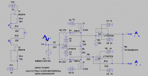
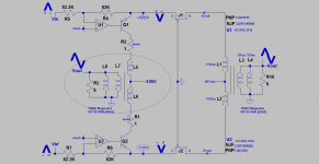
The attached is the complete schematic for the power output stage of a proposed stereo amp using Class aP amplification. The following additional details are for this right channel [arbitrary]. They are fully applicable and/or expected to be identical to those of the forthcoming left channel.
1. Analog pulse music trains are offered to the inverting inputs of the OpAmps [U1 and U2] via the [82.2K ] input resistors. They emanate from the 2 outputs of the Precision Rectifier which precedes this stage. I've added 0.2K to each input resistor [net = 82.2K] because it is the output impedance of the precision rectifier [actually 220 Ohms].
2. Note the active "time lapse" of the analog pulse trains. The upper OpAmp U1 receives pulses for the denoted active time of [0 to t]. The lower OpAmp [U2] receives analog pulses denoted by [t to t1]. The pulses to U2 follow the pulses given to U1, and do not overlap [meaning not in phase] with them.
3. The OpAmps have an "analog pulse" voltage gain = -1; meaning they invert the phase of the signals as shown visually at the source ports of the JFETs.
4. The negative-going voltage signals which appear at the source of a JFET drag its static bias voltage towards ground where its gate sits. This opens the channel of the JFET and admits more current to flow through it from 105 V through the transformer's winding to ground.
5. The two JFETs take alternate turns [aka push pull] to do so during each's active on-time of the pulses. The transformer reconstitutes the bipolar music signal. Note the phase dots on the trafo's windings for it to properly do so.
6. Each JFET is given a low idle current so as to maintain it in the on-state all the time during operation. Done by the OpAmp and PNP as follows.
7. A biasing circuit containing the LEDs generates an adjustable +Vref [via the multi turn 10K pot] for U1 and separately for U2 via its own 10K pot. The OpAmp now operates [additionally] as a non-inverting DC amp for Vref. It amplifies the value of Vref by a factor of ~ two using the established gain equation of Vout at source of JFET = Vref X [1 + 82K/82.2K].
8. Protect the JFET from over dissipation by starting with the highest level of Vref which fully shuts/pinches off its channel. Then slowly and carefully lower the value of Vref while at the destination high voltage of Vds. Sense the value of the drain current as a voltage drop across the 1 Ohm resistor in the collector circuit of PNP.
9. The music power output transformer [VPT24-1040] is a standard AC power line toroid [TRIAD Magnetics] operating in a voltage step-down mode.
I'll move on next to the Left channel of this proposed stereo amp.
Best
Anton
Attachments
Viable idea to double the power output
I sound like the actor Colombo " one more thing/idea" which is shown in the attached schematic. Please note:
1. The use of a second encircled power output transformer [VPT24-1040] at the collectors of the two PNPs.
2. It follows that the source current of JFET = emitter current of PNP that is attached to it = collector current of the same PNP. Might as well harness the clean collector currents of the PNPs to do useful work.
3. Note the use of a second high voltage PSU of -105Vdc for the PNPs.
4. P-MOSFETs maybe substituted for PNPs.
5. The secondary windings of both transformers maybe further connected in parallel [not shown].
6. The secondary windings of each transformer maybe first connected in series [to get the 24 Vac option of the toroid], and then the newly connected secondaries of both transformers are paralleled.
Best
Anton
Attachments
Update..
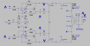
The proto board [1/2 of it] gave me trouble. Several of its insertion points for the right channel became bad. So I assembled a prototype amp on the good 1/2 as the attached schematic shows: Please note the following background which led to it.
1. I only have two SJDP120R085s [from Mr. Pass] for the Right Channel.
2. So I used two UJN1208Ks depletion FETs for the Left Channel.
3. Before I lost the use of 1/2 of the proto board, I was able to match the circuit gain [pulse] for the UJN1208Ks versus one R085.
4. This schematic shows the inverting gain of each OpAmp/UJN1208K circuit was increased by a factor of ~>2.4 to match gain and thus balance the L and R channels [equal volume!]. Said otherwise, the trans-conductance of UJN1208Ks was lower in magnitude than that for the R085s understudy.
5. The pinch-off values for UJNs were also higher in value than those for R085s.
So while I wait for a replacement proto board, this schematic came about and shows:
1. Cascoded UJN1208Ks with the idle R085s as the four FETs are on the same heatsink.
2. Matched the circuit gains of the UJN1208Ks by adjusting the value of OpAmp feedback resistors [199.6K relative to 211.2K so as to get an equal amplitude AC signal [100Hz] at the primary transformer windings TPs [A and B].
3. Then I added Positive Current Feedback [PCF] by using the 1 Meg resistors from the collectors of the PNPs back to the inverting inputs of the OpAmps. This return signal is in-phase with the input pulse signal, and senses the drain current flowing through the FETs.
This transient prototype is stable and sounds great without overall loop feedback. I'll put DC/pulse measurements on its schematic in an upcoming post.
The proto board [1/2 of it] gave me trouble. Several of its insertion points for the right channel became bad. So I assembled a prototype amp on the good 1/2 as the attached schematic shows: Please note the following background which led to it.
1. I only have two SJDP120R085s [from Mr. Pass] for the Right Channel.
2. So I used two UJN1208Ks depletion FETs for the Left Channel.
3. Before I lost the use of 1/2 of the proto board, I was able to match the circuit gain [pulse] for the UJN1208Ks versus one R085.
4. This schematic shows the inverting gain of each OpAmp/UJN1208K circuit was increased by a factor of ~>2.4 to match gain and thus balance the L and R channels [equal volume!]. Said otherwise, the trans-conductance of UJN1208Ks was lower in magnitude than that for the R085s understudy.
5. The pinch-off values for UJNs were also higher in value than those for R085s.
So while I wait for a replacement proto board, this schematic came about and shows:
1. Cascoded UJN1208Ks with the idle R085s as the four FETs are on the same heatsink.
2. Matched the circuit gains of the UJN1208Ks by adjusting the value of OpAmp feedback resistors [199.6K relative to 211.2K so as to get an equal amplitude AC signal [100Hz] at the primary transformer windings TPs [A and B].
3. Then I added Positive Current Feedback [PCF] by using the 1 Meg resistors from the collectors of the PNPs back to the inverting inputs of the OpAmps. This return signal is in-phase with the input pulse signal, and senses the drain current
This transient prototype is stable and sounds great without overall loop feedback. I'll put DC/pulse measurements on its schematic in an upcoming post.
Attachments
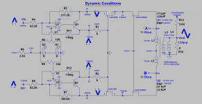
The attached two schematics show the idle and dynamic conditions [entitled] for the prototype amp which I showed in the previous post. Please note:
1. I decreased the high voltage from 105 Vdc to 52 Vdc for this test. By the way, the high voltage PSU is [+/-52 Vdc] of a 75 W/channel unused old receiver. I used 1/2 of it in this instance.
2. The idle current in the FETs is ~30 mA. Its magnitude affects the value of the amp's open loop voltage gain. A higher FET idle current gave a higher open loop gain; say by going from 10 mA to 50 mA idle.
3. The open loop gain of the amp as written is 25 at 100 Hz.
4. The closed loop gain of the amp as written is 11 at 100 Hz.
5. Please go to post #148 which showed the connection of overall negative feedback. It emanates from the secondary of the power output transformer [TRIAD] via the resistor [5.6K] to the inverting input of the front end OpAmp [OPA134] of the Precision Rectifier. Beware of improper phasing of the feedback signal. The other-way attachment [positive voltage feedback] will cause the amp to oscillate. The color coding of the TRIAD's primary and secondary leads is your guide for proper connection.
6.The amplitude of a measured analog pulse is preceded with a [+ or -] to signal positive or negative going; like further shown by the apex direction of the aP graphics. A [p] sign post its measurement signified pulse. They were scope measurements.
7. The reconstituted AC signal [100 Hz] happens at the Blue and Brown primary leads of the TRIAD. The magnitude of the now AC signal has a post [p-p] sign to mean peak to peak. AC signals were also scope measurements.
This amp is stable against oscillation. I'll raise the high voltage to ~105 Vdc, and listen to it with and without overall negative feedback. I'll post a comment on subjective performance.
Attachments
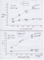
Objective and Subjective [musical] performance of Class aP[UJN1208K]
The attached picture shows two plots which correlate the voltage gain of the Class aP power amp [previous post] as a function of the amp's quiescent conditions.
Figure 1. Please note that the load is 8 Ohms across the secondary leads of the [TRIAD] power output transformer which is rated at 25 VA. The voltage gain results are recorded on the plots. The previous post also showed my definition of the amp's voltage gain and the application of overall negative feedback. Test frequency was 100 Hz.
1. Open loop voltage gain [OLV] increased in magnitude from an average of 13 to ~ 35 due to an increase in the idle [bias] of the FETs from 10 to 50 mA.
2. The value of the high voltage [B+] of 52 V or 105 V showed a trivial effect on OLV; because UJN 1208K is cascoded.
3. Closed loop gain [CLV] changed between 7.5 to 13 in the same range of current flowing through the FETs.
Figure 2 Please note the value of the new load [16 Ohms] across the the secondary output leads of the trafo. I only used one value for B+ = 105 V.
1. OLV increased from 23 to 72 due to increasing FET current from 10 to 50 mA as in Figure 1. The trafo is 25 VA TRIAD .
2. OLV decreased to 64 [excuse my error in the written triangle data point] when a 100 VA TRIAD trafo was used instead the 25 VA TRIAD trafo. Both trafos have the same voltage step-down ration of 10:1.
3. CLV changed between 10 and 16 due to the FETs' current change of 10 to 50 mA using the 25VA power output transformer.
Musical performance.
The input of the precision rectifier was fed a musical signal from the headphone output of a Marantz CD player which has a manual volume control. The secondary winding of the opt trafo energized a 6-Ohm rated ADS L730 loudspeaker to a satisfactory volume .
1. Performance with CLV was better than that with OLV [duh..] using either the 25VA or the 100 VA TRIAD opt.
2. Performance with CLV and the 100 VA trafo was substantially better than that from the 25 VA trafo. It was robust detailed and spacious top to bottom. The system was light on its feet and sounded great.
3. OLV performance was also better by using the 100 VA than the 25 VA opt. The 25 VA trafo amp gave the impression of behaving more like a current than a voltage source driving the ADS .
This Class aP approach is viable, controllable and easy to implement; with a similar application potential using vacuum tubes cascoded with SIC depletion or enhancement FETs. I will lay off posting in this thread for a while. I'll be back.
Best
Anton
Attachments
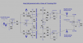
Class aP Signal-Tracking Bipolar Power Supply Unit [PSU]
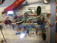
The photo of the prototype PSU is attached. It is assembled on a prototyping board. Its detailed schematic is also attached. A second scope photo shows a 20 KHz sine signal. It is ~16 Vp-p at Vout of [U4] which is the device under test [DUT].
Class aP is a natural approach for this application. Because it embodies accurate timing and phase for the processed signals. Here's how it works:
1. The left side of the $ sign vertical barrier shows an OpAmp [1/2 OPA2134] used as a buffer for its 20 KHz [Vin] signal. Its output drives the inverting input of its twin which operates as a Precision Rectifier [PR].
2. The two outputs of [PR] are analog pulses. One is positive-going and is separated from the other which is negative-going. Note the notation of timing [0 to t and t to t1] on each analog pulse; so as to correlate with that of the input signal.
3. The middle section of the schematic [sandwiched between the $ and * vertical barriers] shows two independent summing OpAmp inverters. Each inverter sums its requisite analog pulse and a fixed reference voltage which is derived from an LED.
4. The output of this pair of OpAmp inverters [U2 and U3] is the Tracking Bipolar PSU. Has proper timing and phase. The output of the upper OpAmp [U2] has a very low output impedance. It shows a reference [-2.7 Vdc] upon which rides a negative-going pulse. The output of the lower OpAmp [U3] also has a v.low output impedance. It shows a positive-going analog pulse riding atop a [+2.7Vdc] reference.
5. The +/-2.7Vdc outputs of [U2 and U3] go the power pins of the DUT. This is the idle PSU.
6. The DUTs test were OPA134 , LF356N [in photo] and uA741. uA741 was not happy!.
7. The DUT operates as a buffer and is driven by the same [Vin input] signal at its non-inverting input.
8. Vout of DUT has the same ~magnitude and shape as Vin input. Proof positive of tracking.
I'll resume in a second post before the system times me out.
Attachments
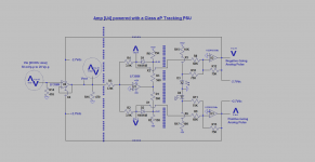
A Class aP tracking bipolar PSU
The previous post demonstrated the feasibility of this tracking PSU concept on a flea-power OpAmp. This post explains the operation of the device under test [DUT which is still an OpAmp] energized by this tracking bipolar PSU. The longer term objective is to use in practical power amps.
The attached schematic is like that I showed in the previous post. I unraveled the power output stage of the target OpAmp [U4] to help clarify operation.
1. U4 and its power output stage are shown as a generic model at the far right of the schematic.
2. The model output stage is a BJT of complementary symmetry.
3. Focus on NPN. As the output AC signal voltage on its emitter rises and falls during its duration of [0 to t seconds], its collector [already at an idle +2.7 Vdc] experiences a positive-going analog pulse during its same time duration of [0 to t seconds].
3a. It follows that the collector to emitter voltage of NPN [Vce] stays put at [+2.7 Vdc]. NPN is active [amplifies] during the [0 to t] duration and its power dissipation is minimized. Operation at a constant Vce of NPN is also called cascoding it.
3b. During the amplifying time interval of the output AC signal [at the emitter of NPN] and its positive-going analog pulse [at NPN collector] of [0 to t seconds], PNP is not active. Its collector voltage resides at its idle [-2.7 Vdc] because its negative analog pulse is not present and is in the future [t to t1 seconds].
3c. The Vce of PNP is not constant; because its collector is at a constant [-2.7Vdc] but its emitter is simultaneous going positive from the output signal. Still its power dissipation is minimized because of its initially-low idle collector voltage.
4. The above discussion [operation] in points [3 to 3c] is readily repeated for PNP during the time duration of [t to t1 seconds ] of the AC output signals and its simultaneous negative-going analog pulse.
More to come...
Best
Anton
Attachments

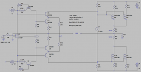
Case of a bootstrapped Class aP tracking bipolar PSU
The attached schematic shows the OpAmp [LF356N; U4] using its output signal to power a Class aP bipolar tracking PSU so as to generate its power supply rails.
Here' how it works by using an example 20 KHz output signal spanning a voltage range of [50 mVp-p to 20Vp-p]. That it works this well is a testament to the high quality OpAmps understudy and the genius of their makers.
1. OpAmp [U4] operates as a buffer example. It is to the left of the star vertical barrier.
2. Its output drives a following Precision Rectifier [PR] which is sandwiched between the $ and star signs vertical boundaries. It has been discussed in past posts. The OpAmp used therein is LF356N; but it may well be a newer state of the art OPA134 or other. Its two outputs are separate positive-going and negative-going analog pulses. Each starts and ends at a ~few millivolts of 0 Vdc.
3. The positive-going analog pulse from [PR] and a positive voltage reference of [+2.7 Vdc from LED] are summed at the inverting input of its requisite OpAmp [1/2 OPA2134]. Its output is [-2.7Vdc] atop which rides a negative-going analog pulse [meaning it is heading towards -15 Vdc]. This output is the bootstrapped and tracking negative PSU rail for U4 . It folds or is sent back to the front end U4; thus the appropriate use of the noun bootstrap!
4. The negative-going analog pulse from [PR] and a negative voltage reference of [-2.7Vdc fro a second LED] are summed at the inverting input of its requisite OpAmp [a second 1/2 OPA2134 of the above]. Its output is [+2.7Vdc] atop which rides a positive-going analog pulse [meaning its peak voltage is heading towards +15Vdc]. This is the output which is a bootstrapped and tracking positive PSU rail for U4. It folds or is sent back to the front end U4 which allows using the noun bootstrap.
5. The operation or works of the simple tracking PSU of the previous post and the bootstrapped bipolar PSU tracker of this post are different in a subtle manner.
LM3886 is a popular Class AB power chip which requires a minimum +/-10 Vdc to operate. Someday it maybe used like U4 [but with voltage gain] in the attached schematic or preferably a simpler one [forthcoming] to chase this direction.
Best
Anton
Attachments
Relevant information for a Tracking Bipolar PSU
May I direct your attention to the thread in the Solid State Forum which is entitled "The Blomley Class B amplifier" by DIYer revenant. Please note the schematic in post #29. It is a special Class aP power amplifier. Here are its details:
1. The evident generous and expert contribution of Mr. Ian Hegglun; both in LTSpice and Electronics to include using his configuration for the power output stage.
2. The front-end Precision Rectifier [PR] using 2N390X BJTs. Its outputs are separate positive and negative-going analog pulses which are referenced to the power rails instead of common. Positive-going means that the peak of its pulse is heading to common from its negative power rail origin. Negative-going means that the peak of its pulse is also heading towards common but from its positive rail origin.
3. Hegglun's schematic may well be the basis for a high quality and high power Class aP tracking bipolar PSU.
4. I have experimented with the attached schematic of an actual Class aP amplifier prototype. It is also expected to be useful like that of Hegglun's. I'll find its post in this thread and direct you to it.
Best
Anton
Attachments
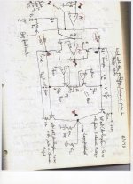
May I direct your attention to post #144 in this thread. Its attached schematic [a working .asc file] shows a Class aP power amp which is like that in the previous post; except that it uses a complementary TIP120/ TIP125 power output stage. It is expected to be usable in/as a Class aP tracking bipolar PSU.
The two attached scans of my notebook show that this approach for a Class aP power amp is ~20 years old. I still have the power output complementary MOSFETs and the BJTs on individual heat sinks.
I need to meditate on the practical value of the front-end buffer; OpAmp [A1] in the right scan. Note the origin of its feedback loop.
Best
Anton
Attachments
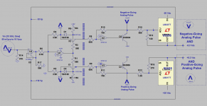
A Class aP tracking bipolar PSU using LM317T and LM337T
The attached schematic shows a Class aP bipolar tracking PSU [+/-18 Vp] which uses LM317T and LM337T voltage regulators. They are positive and negative voltage regulators respectively. Please note:
1. Each regulator was configured to deliver a fixed and idle /8.3/ Vdc by using the circuit and equation in its application notes. The output resistor string which determines this idle output voltage was referenced to the output of the target OpAmp rather than to ground.
1a. Essentially the target OpAmp "lifts" the said resistor string towards +15 V [for LM317T] and -15V for LM337T during its active time interval [ e.g. 0 to t seconds].
2. A 2N390x/y BJT buffered the target OpAmp. It bypassed the sizable current flowing though the regulator's external resistor string to its collector's destination of [+/-15 Vdc].
3. The tracking bipolar PSU is stable against oscillation at both idle and when energized with/by the corresponding analog pulses. The outputs of the regulators were separately loaded [not shown] with light bulbs [5W] . Each drained ~ 50 mA at idle from each regulator.
4. The resultant tracking bipolar PSU rails were returned to the front end OpAmp buffer [LF356N]. This qualifies this application as a bootstrapped tracking bipolar PSU. The output of LF356N was further loaded with 560 Ohms which had a 16 Vp-p at 15 KHz signal across it. This added to the idle current consumption of the regulators.
5. LM317T did better at 20 KHz compared with LM337T which did its best at 15 KHz. I eye-balled the quality of the half-sine analog pulses as the method to determine this. The remedy was to decrease the input voltage until the quality of the analog pulses for both outputs was presentable.
6. The regulators have short-circuit and over temperature protection which is beneficial.
7. Another approach is to use a Zener which is driven by a constant current source tied to the respective high voltage rails [+/-20 Vdc].
7a. One end of the Zener goes to the output of the target OpAmp [BJT emitter] which would move it towards its prescribed [+/-15 Vdc] rails like that done for the regulators' resistor strings.
7b. The Zener's output [Vz] then drives the gate of a high power MOSFET configured as a follower affixed to a heat sink like I did for the voltage regulators.
Next will be a tracking bipolar PSU for rail voltages >18 Vp.
Best
Anton
Attachments
- Home
- Amplifiers
- Pass Labs
- Class aP amplification