I dislike the name SIT.
Didn't Nishizawa the inventor call them "SIT"s in his published papers?
Didn't Nishizawa the inventor call them "SIT"s in his published papers?
BAM https://iopscience.iop.org/article/10.7567/JJAPS.17S1.231/pdf
Original patent 1972
https://patentimages.storage.googleapis.com/88/11/72/d729c179b87c10/US3828230.pdf
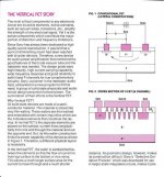
Fig 7 shows permeable buried gate
Patent abstract mentions triode behavior
https://patentimages.storage.googleapis.com/88/11/72/d729c179b87c10/US3828230.pdf
Fig 7 shows permeable buried gate
Patent abstract mentions triode behavior
But a JFET is not a MOSFET.
Certainly not. It is a vertical FET, but far from an "ordinary" vertical FET. Simply using pure silicon dioxide would have resulted in insufficient conductivity, thus a nonfunctional transistor. Otherwise, the lateral structure in itself produces lower distortion than the vertical structure.
Didn't Nishizawa the inventor call them "SIT"s in his published papers?
Right, now I remember, he made the invention around 1950. Great principle and technology (25 years later).
Frankly, I don`t know who came up with the lofty name Static Induction Transistor, maybe some semiconductor professor.
I have read that it was Nishizawa himself who came up with SIT name
(you are right he was a famous professor), and they were referred to as
VFETs until vertical Mosfets (like the IRF240) came to dominate the
marketplace, and the VFET name became confusing, and was largely
abandoned with reference to SITs.
We audiophiles still have affection for VFETs from the old days of Sony
and Yamaha. I agree that the whole thing is somewhat confusing.
And it's a junction device, not a Mosfet - I can measure the current going
through the Gate, something you will not see on a Mosfet. There are
apparently now examples of SITs operated as bipolar transistors, not
that I find it attactive...

")
The day may come when
you have to choose between a noisy SIT and a new replacement semiconductor.
I wonder how many years we can expect a SIT would last under high temp (or high current) condition in class-A amps. It seems many original VFET amps by Sony and Yamaha are affected by dead original SIT, and they are not even biased class-A. Their heatsinks look rather tiny, though.
PS: I have an impression that SITs are very robust, and my ones are all still survived after stupid mistakes that I made.
Last edited:
I am using Sony TA 5650- TAN 8550 - after doing those replacement of death diodes / other suggested modifications. They are working beautifully. Many such modified units are working well - see Audiokarma site. Nothing wrong with V-Fets. Any power semiconductor can go bad - Murphy's law! That does not deter people from building amplifiers and using them. In fact Yamaha B2 amplifiers work even with bad treatments without doing any modifications.
They also sound fantastic in Class AB
They also sound fantastic in Class AB
Well, it is easy to feel disoriented in the conceptual, definitional and naming mess of physics. What is alluded to as PN junction is an essential and central element of all semiconductors with or without a gate insulation film.
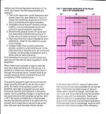
The excellence of the Sony V-FET decisively lies in the electrically and technically unique gate-source interface. The PN junction determines the transfer characteristics as well as the threshold voltage. Typically, the depletion region in a PN junction is very thin, yielding a low threshold voltage, a large transconductance and huge interelectrode capacitances. Because of its high resistance, almost the entire bias voltage appears across the depletion region.
An oxide layer can be implanted between the gate electrode and the semiconductor. What is unique to the Sony V-FET is the exceptional thickness and material purity of the oxide layer. Constituting a series capacitance, the oxide layer reduces the capacitance of the PN junction and raises the gate to channel voltage. The nominal gate to channel voltage of the 2SK60 at 100mA is -18V (can even be as high as -25V), the input capacitance at Vgs -15V is 190pF and a small reverse transfer capacitance can safely be assumed. The buried gate is diffused in the doped regions and the low series resistance permits considerable gate currents. Applying a forward bias voltage to any depletion mode device is a bad practice. A heavier load requires larger driving amplitudes and preferably a driver stage with voltage amplifying ability.

res07njc,
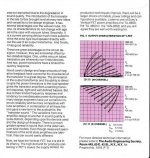
the depletion layer controls the conducting channel and transition consistency. A short channel length is hard to control and more prone to velocity saturation. Since the voltage to current relationship is nonlinear, there is no way to define the resistance for a PN junction, however, it is reflected in the threshold voltage. The high threshold voltage of the Sony and Yamaha devices suggests a high resistance layer, that is, a high built-in electrostatic potential. The reverse bias provides appropriate channel control by restricting the channel thickness and augmenting the depletion layer. No current source.
the depletion layer controls the conducting channel and transition consistency. A short channel length is hard to control and more prone to velocity saturation. Since the voltage to current relationship is nonlinear, there is no way to define the resistance for a PN junction, however, it is reflected in the threshold voltage. The high threshold voltage of the Sony and Yamaha devices suggests a high resistance layer, that is, a high built-in electrostatic potential. The reverse bias provides appropriate channel control by restricting the channel thickness and augmenting the depletion layer. No current source.
- Home
- Amplifiers
- Pass Labs
- Firstwatt SIT noise issues?