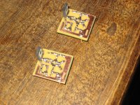
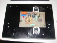
Here's a photo of the boards with all SMD components on, as well as the MJE243s and the mounting pins (mostly invisible because they're on the bottom, obviously. Connections to this little board are for input, positive rail, base and emitter of the MJE243, from R6 (which is SMD) and to R4 (which is not - will be as close as I can get it to the agte of the mosfet). I hope all the resistors are OK as SMD - the one I'm most concerned about is R1; I drew the boards and put it on reckoning that the power rating would be OK, but now I'm not sure. How do you calculate the voltage across it? Do you need the gate voltage of Q3 first? (Sorry if this is another dumb question - I'm learning this stuff as I go along.)
I'm off to buy metal and nuts and bolts and things for a chassis this morning, and will also try to get a hold of some motor run caps to try.
Cheers
Nigel
I'm off to buy metal and nuts and bolts and things for a chassis this morning, and will also try to get a hold of some motor run caps to try.
Cheers
Nigel
Attachments
.... the one I'm most concerned about is R1;...
How do you calculate the voltage across it? ...
Ohm's Law !


Q1 (CCS) supplies 18ma - every BF862 in LTP gets 9ma, so the same current (9ma) runs through R1.
V = R * I = 470 * 0.009 = 4.23V
P = I * I * R = 9mA * 9ma * 470R = 38 mW
If you get a lot of DC on the output, try lowering R7 down to 0R22, and adjust the DC offset with R12 (R12 should be a 100R pot).
Don't run more than 10mA through Q2 (4.7V on R1). And if you can't set DC offset to zero with 10ma or less (through Q2) use 560R for R1. (Everything depends on Q3's Vgs at desired Id, which is 1A to 1.3A - you'll have to pick the value by experiment, try with 1A first - use 0R68 for R16)
Last edited:
Hi Juma,
Thanks for the answer - do you mind a couple of follow-up questions?
I'm quite comfortable with all the calculations once I know the current through R1. I had been trying to figure this out differently, by considering the voltages around Q3, but your explanation is very clear, except for two things.
1. You mentioned once before the same fact you used here - that the current through Q1 is 18mA. But why is this the case? Do I understand correctly that L1 creates a voltage difference between the base and emitter of Q1 (which is fine-adjusted by R12), which causes this current? If so, how do we get the specific value of 18mA?
2. Where does this current that enters the LTP go, and in what proportions? Some of the current through Q2 goes through R1 and some through R4, but Q5 goes straight to the rail. How much current goes through R4? (Again, if I know the voltage at the gate of Q3 then I can calculate this, no problem, but that was where I was stuck...)
A few more questions here too.
3. Above somewhere you suggested raising the 0R5 resistors (I presumed you meant both R7 and R16) to 0R66 if the bias, and heatsink temp, were too high. So wouldn't your suggestion of lowering R7 raise the bias current, and hence the heatsink temp? (I'm not saying this is necessarily a bad thing- just to understand...)
4. Your remark about Q3's Vgs is exactly where I was trying to start to calculate the voltage across R1. How do we get this? Just by experiment with the particular mosfet?
5. When you say 0R68 for R16, what about R7? Is it just coincidence that in the schematic the values are both 0R5, or is it better for them to be equal values? This is an important point I don't understand, perhaps - above ZenMod stressed I should use the same mosfet for Q3 and Q6, which suggests things should be symmetrical for R7 and R16 also, right? This makes sense to me if the idea is to keep DC offset around R19 as close to zero as possible.
OK, many thanks for any explanations you have time for.
Cheers
Nigel
Thanks for the answer - do you mind a couple of follow-up questions?
Ohm's Law !
Q1 (CCS) supplies 18ma - every BF862 in LTP gets 9ma, so the same current (9ma) runs through R1.
V = R * I = 470 * 0.009 = 4.23V
P = I * I * R = 9mA * 9ma * 470R = 38 mW
I'm quite comfortable with all the calculations once I know the current through R1. I had been trying to figure this out differently, by considering the voltages around Q3, but your explanation is very clear, except for two things.
1. You mentioned once before the same fact you used here - that the current through Q1 is 18mA. But why is this the case? Do I understand correctly that L1 creates a voltage difference between the base and emitter of Q1 (which is fine-adjusted by R12), which causes this current? If so, how do we get the specific value of 18mA?
2. Where does this current that enters the LTP go, and in what proportions? Some of the current through Q2 goes through R1 and some through R4, but Q5 goes straight to the rail. How much current goes through R4? (Again, if I know the voltage at the gate of Q3 then I can calculate this, no problem, but that was where I was stuck...)
If you get a lot of DC on the output, try lowering R7 down to 0R22, and adjust the DC offset with R12 (R12 should be a 100R pot).
Don't run more than 10mA through Q2 (4.7V on R1). And if you can't set DC offset to zero with 10ma or less (through Q2) use 560R for R1. (Everything depends on Q3's Vgs at desired Id, which is 1A to 1.3A - you'll have to pick the value by experiment, try with 1A first - use 0R68 for R16)
A few more questions here too.
3. Above somewhere you suggested raising the 0R5 resistors (I presumed you meant both R7 and R16) to 0R66 if the bias, and heatsink temp, were too high. So wouldn't your suggestion of lowering R7 raise the bias current, and hence the heatsink temp? (I'm not saying this is necessarily a bad thing- just to understand...)
4. Your remark about Q3's Vgs is exactly where I was trying to start to calculate the voltage across R1. How do we get this? Just by experiment with the particular mosfet?
5. When you say 0R68 for R16, what about R7? Is it just coincidence that in the schematic the values are both 0R5, or is it better for them to be equal values? This is an important point I don't understand, perhaps - above ZenMod stressed I should use the same mosfet for Q3 and Q6, which suggests things should be symmetrical for R7 and R16 also, right? This makes sense to me if the idea is to keep DC offset around R19 as close to zero as possible.
OK, many thanks for any explanations you have time for.
Cheers
Nigel
Voltage drop over LED1 is 1.7V with couple of mA through it (supplied by Q4). Vbe on Q1 is physical constant (about 0,65V - constant for any BJT). So we have about 1V on R1. Since voltage on Q1's base is constant so is the current through R1 and Q1 (I=V/R=1V/56R=17.8mA) - that's why it's called constant current source (CCS)....
1. You mentioned once before the same fact you used here - that the current through Q1 is 18mA. But why is this the case?
CCS supplies LTP through sources of JFETs. Q2 and Q5 share that current in accordance with their characteristics (that's why we match them sometimes) and R10 and R11 help in equalizing that sharing (they also degenerate sources od JFETs and lower the gain of LTP). R4 is posing as drain load for Q2 and voltage drop over R4 is Vgs of Q3. Vgs determines the Id through Q3.2. Where does this current that enters the LTP go, and in what proportions? Some of the current through Q2 goes through R1 and some through R4, but Q5 goes straight to the rail. How much current goes through R4? (Again, if I know the voltage at the gate of Q3 then I can calculate this, no problem, but that was where I was stuck...)
Q6 and Q8 form the CCS too - enough spoon-feeding, figure out how does it work (mind C3 and R22 - tip: Zen 2 article, figure 6.)3. Above somewhere you suggested raising the 0R5 resistors (I presumed you meant both R7 and R16) to 0R66 if the bias, and heatsink temp, were too high. So wouldn't your suggestion of lowering R7 raise the bias current, and hence the heatsink temp? (I'm not saying this is necessarily a bad thing- just to understand...)
Q3 is an amplifier and R7 is just it's source degeneration resistor
Datasheet gives you that, but there are tolerances, not all parts are created equal4. Your remark about Q3's Vgs is exactly where I was trying to start to calculate the voltage across R1. How do we get this? Just by experiment with the particular mosfet?
R16 sets the current through Q6 and Q3, R7 is not that important. Zen Mod recommended using same MOSFETs for Q3 and Q6 from the reasons connected with Aleph current source - it does some kind of amplifying too5. When you say 0R68 for R16, what about R7? Is it just coincidence that in the schematic the values are both 0R5, or is it better for them to be equal values? This is an important point I don't understand, perhaps - above ZenMod stressed I should use the same mosfet for Q3 and Q6, which suggests things should be symmetrical for R7 and R16 also, right? This makes sense to me if the idea is to keep DC offset around R19 as close to zero as possible.
There will be no DC offset if you properly set the current through both MOSFETS, and now you know how to do that.Once again - all Mr. Pass' articles are very educational and informative, find the time to study them, you'll be surprised how much you can learn reading them...
Thank you very much, juma, that's really very clear. I am reading the zen articles, as you suggested, so between the PassDiy lessons and your (and ZenMod's) explanations I will slowly understand things better. And of course, if I end up with a nice-sounding amplifier and have fun doing it then what more could a hobbyist want?
No luck on the motor run caps, yet, by the way - maybe better to talk to a local repairman than to the people in the parts shop...
Anyway, back to hacksawing aluminium...
Many thanks again
Cheers
Nigel
No luck on the motor run caps, yet, by the way - maybe better to talk to a local repairman than to the people in the parts shop...
Anyway, back to hacksawing aluminium...
Many thanks again
Cheers
Nigel
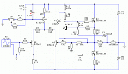
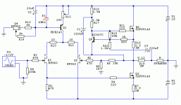
Curiosity got better of me so I spent few hours last weekend to build one channel (point-to-point) of this amp to test it and it works fine. Here is the schematic (some values changed, closer to what Mr. Pass used in Aleph-J).
All caps are polarized properly in this sch. and it's more legible that the previous one
I used IRFP9140 (1.25A bias) in output stage with no ill effects, at least not in what you can hear on one channel. Current through R1 was 9.2mA. PS was +/-18.5 V unregulated. JFETs do get hot but not too hot - they played music for couple of hours without problems. (Tip: JFETs gate dissipates most of the heat and that should be taken into account when making a PCB layout).
I'm sure that njepitt will do more critical listening, but I can bet that there is no need to chase (almost) unobtainable 2sj109 or matched 2sj74, equally good amp can be made with easy to find BF862 and P-channel MOSFETs in output stage (and it's possible that some people might prefer the IR parts).
Attachments
Curiosity got better of me so I spent few hours last weekend to build one channel (point-to-point) of this amp to test it and it works fine. Here is the schematic (some values changed, closer to what Mr. Pass used in Aleph-J).
All caps are polarized properly in this sch. and it's more legible that the previous one
I used IRFP9140 (1.25A bias) in output stage with no ill effects, at least not in what you can hear on one channel. Current through R1 was 9.2mA. PS was +/-18.5 V unregulated. JFETs do get hot but not too hot - they played music for couple of hours without problems. (Tip: JFETs gate dissipates most of the heat and that should be taken into account when making a PCB layout).
Hi juma,
Interesting - glad to hear it works, although I really never doubted it. I'm wondering why you changed some of these values - was it by experimentation, or did you have some more theoretical reason? I'm particularly interested in R2 and R3, which have been changed from 220R to 470R, since these will be the hardest of your changes for me to do (since are SMD on my little boards...) I will probably leave them as they are for the time being. The rest will be p2p for me too, so I can play around more easily with these values...
Incidentally, I managed to get my hands on IRFP9240's so I will probably use these and save the IRFP9140 for something else.
I'm sure that njepitt will do more critical listening, but I can bet that there is no need to chase (almost) unobtainable 2sj109 or matched 2sj74, equally good amp can be made with easy to find BF862 and P-channel MOSFETs in output stage (and it's possible that some people might prefer the IR parts).
I'm equally sure that if my amp doesn't meet expectations the fault will be with my build, not the schematic...
Thanks again for the input
Cheers
Nigel
There's nothing wrong with first schm., it's just that I wanted to approximate Mr. Pass' Aleph-J, since I didn't build it before.I'm wondering why you changed some of these values - was it by experimentation, or did you have some more theoretical reason?
Leave it as it is, those are least significant parts, they can be anything from 47R to 2k or moreI'm particularly interested in R2 and R3, which have been changed from 220R to 470R...
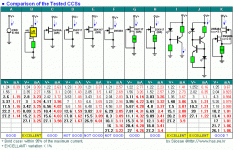
Juma - two bjt CCS will give somewhat more stable output offset ;
not must , but just a possibility
IME red LED referenced CCS is more stable than one with 2 BJTs.
Walt Jung wrote about it here: http://waltjung.org/PDFs/Sources_101_P1.pdf
(compare figures 3B and 5B and note that W.J. used green LED which is inferior to red LED)
Here is another CCS test (column "I"):
Attachments
Last edited:
Finished and playing!
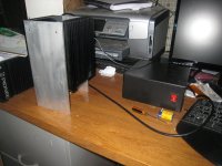
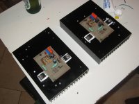
So I have finished the amp, and am listening to it as we speak. I have attached three photos, showing the heatsinks with boards attached, and the amp and its power supply. First impression is that it sounds great, but for non-audio reasons my subjective opinions shouldn't be trusted this evening, since I had an ear-doctor's appointment today, and as a result everything (car alarms, breaking china, screaming children, as well as music) all has an "enhanced treble".... but in a good sense A few days will clear this false perspective, and I can give you a more realistic report on how it sounds.
I can give you some numbers, however, for those who care. The power supply is giving me marginally more than +/- 18VDC - measured as +18.3 and - 18.0 with the amplifier cold and before adjustments. I used 0.46R resistors for R7 and R16, and am getting 0.57V across R7 (on both channels) which makes a bias current of 1.24A - right about where we want it. I also measured voltage across R10 (107.5mV on both channels, exactly!) and across R11 (93.3mV on one channel, 96.2mV on the other) which gives close to 10mA on each half, as juma explained above. As far as heat goes, I have been listening for a little over an hour, with ambient temp around 27 celsius, and the heatsinks are measuring 50-51 degrees C. (Not at the tip of the fins, but pushing the probe in so it is touching the aluminium right behind where the mosfet is - that is, the hottest part.)
I have a couple of queries about heat, though.
1. I have always sanded off the anodizing from heatsinks where the mica (and the mosfet above it) will touch, since Iread somewhere (maybe the ESP site) that this is advisable. This time I didn't do that, partly because I was in a hurry, and partly because sanding off the anodizing always creates slight irregularities in the surface, which is bad. Do most people here sand the black off? Or don't worry about it?
2. The little BF862 jfets are hot. I didn't put any heatsinking on them (or on the MJE243, which is also hot) but I can put my finger on them for about 4-5 secs (and it doesn't burn, although does hurt...). Anything to worry about? I should add, I didn't glue any copper on as I mentioned above because my final design for the little PCB left very little space. (Pathetic excuse, I know...) If I were doing this again (as I well might, who knows?) I think I would follow juma's suggestion and use a little board space to help with this. Meanwhile, does anyone think this is a disaster waiting to happen? Or I shouldn't lose sleep over it?
Many thanks again for all advice. I have to go - Elisabeth Schwarzkopf is calling...
Cheers
Nigel
So I have finished the amp, and am listening to it as we speak. I have attached three photos, showing the heatsinks with boards attached, and the amp and its power supply. First impression is that it sounds great, but for non-audio reasons my subjective opinions shouldn't be trusted this evening, since I had an ear-doctor's appointment today, and as a result everything (car alarms, breaking china, screaming children, as well as music) all has an "enhanced treble".... but in a good sense
A few days will clear this false perspective, and I can give you a more realistic report on how it sounds. I can give you some numbers, however, for those who care. The power supply is giving me marginally more than +/- 18VDC - measured as +18.3 and - 18.0 with the amplifier cold and before adjustments. I used 0.46R resistors for R7 and R16, and am getting 0.57V across R7 (on both channels) which makes a bias current of 1.24A - right about where we want it. I also measured voltage across R10 (107.5mV on both channels, exactly!) and across R11 (93.3mV on one channel, 96.2mV on the other) which gives close to 10mA on each half, as juma explained above. As far as heat goes, I have been listening for a little over an hour, with ambient temp around 27 celsius, and the heatsinks are measuring 50-51 degrees C. (Not at the tip of the fins, but pushing the probe in so it is touching the aluminium right behind where the mosfet is - that is, the hottest part.)
I have a couple of queries about heat, though.
1. I have always sanded off the anodizing from heatsinks where the mica (and the mosfet above it) will touch, since Iread somewhere (maybe the ESP site) that this is advisable. This time I didn't do that, partly because I was in a hurry, and partly because sanding off the anodizing always creates slight irregularities in the surface, which is bad. Do most people here sand the black off? Or don't worry about it?
2. The little BF862 jfets are hot. I didn't put any heatsinking on them (or on the MJE243, which is also hot) but I can put my finger on them for about 4-5 secs (and it doesn't burn, although does hurt...). Anything to worry about? I should add, I didn't glue any copper on as I mentioned above because my final design for the little PCB left very little space. (Pathetic excuse, I know...) If I were doing this again (as I well might, who knows?) I think I would follow juma's suggestion and use a little board space to help with this. Meanwhile, does anyone think this is a disaster waiting to happen? Or I shouldn't lose sleep over it?
Many thanks again for all advice. I have to go - Elisabeth Schwarzkopf is calling...
Cheers
Nigel
Attachments
Hey, great job on those! I don't think the little JFETs should get that hot. I don't know how much power they are dissipating, but the hotter they are the less power they can handle. I think they are 350mW devices.
Maybe the associated circuitry is making them hot? If not you may need to make some adjustments to circuit or add heatsinks. Though they are pretty small and kind of hard to put effective heat sinking on.
Maybe the associated circuitry is making them hot? If not you may need to make some adjustments to circuit or add heatsinks. Though they are pretty small and kind of hard to put effective heat sinking on.
....does anyone think this is a disaster waiting to happen? Or I shouldn't lose sleep over it? ...
Hi Nigel, i'm glad you made it work as predicted
BF862 is dissipating most of the heat through Gate pin. You can make a thin copper "fin" (1 or 2 square inches) and solder it very close to the Gate pin. That will improve cooling of JFETs (and your sleep too
)Right now your JFETs are dissipating about 190mw and datasheet tells us that each of them can take 300mW up to 90 deg.C
MJE243 gives you numerous heatsinking options, but I wouldn't bother (it's too big a BJT to be scared by mere 360mw of Pd)
Happy listening
*************************************
Now I see that I made a mistake in post #46 - Drains of JFETs are marked as Sources.
Here is the corrected schematic:
Attachments
Last edited:
Nigel, one more thing:
looking closely to the 2nd of your pics in post #51 (mini PCB detail), it seems to me that one of your LTP JFETs is upside down (Drain interchanged with Source).
Please check it, although JFETs have that wondrous property (D & S are pretty much interchangeable)
looking closely to the 2nd of your pics in post #51 (mini PCB detail), it seems to me that one of your LTP JFETs is upside down (Drain interchanged with Source).
Please check it, although JFETs have that wondrous property (D & S are pretty much interchangeable)
Attachments
Nigel, one more thing:
looking closely to the 2nd of your pics in post #51 (mini PCB detail), it seems to me that one of your LTP JFETs is upside down (Drain interchanged with Source).
Please check it, although JFETs have that wondrous property (D & S are pretty much interchangeable)
juma: Actually, the data sheet says that they are *really* interchangeable in this case, so I used that in the design of the pcb. I should add that I also matched them according to how they would be on the board, that is, switching d and s appropriately. Do you think it matters? (Again, this isn't something I can change easily on *this* board, but if I ever rebuild it could be taken into account.)
I'm thinking about how to put on a little copper fin as you suggest... that pcb is pretty small, and the gate pin is tiny... hhhmmmmm...
Any thoughts on sanding off the anodizing on the heatsink?
Cheers
Nigel
Obviously not, if it behaves OK, then it's OKjuma: Actually, the data sheet says that they are *really* interchangeable in this case, so I used that in the design of the pcb. I should add that I also matched them according to how they would be on the board, that is, switching d and s appropriately.
Do you think it matters?
Leave the anodizing - some are even using it (successfully) instead of mica insulator. Sanding it off might cause more problems than benefits (in terms of heat transfer). Anyway, 50-51 deg.C behind the MOSFET is a nice figure, leave it alone...Any thoughts on sanding off the anodizing on the heatsink?
I'm thinking about how to put on a little copper fin as you suggest... that pcb is pretty small, and the gate pin is tiny... hhhmmmmm...
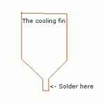
Your "fin" should look something like this (see the pic). Take the thin copper tin, cut it with scissors, solder it and fold it the way it suits your PCB
Attachments
Obviously not, if it behaves OK, then it's OK
Sounds OK (at least to yesterday's ears..) Whether it measures OK or not is another question, although much less important.
Leave the anodizing - some are even using it (successfully) instead of mica insulator. Sanding it off might cause more problems than benefits (in terms of heat transfer). Anyway, 50-51 deg.C behind the MOSFET is a nice figure, leave it alone...
OK. Actually, it got up to 53 deg. C, but that's still OK. In hotter weather I might have to reconsider this.
Your "fin" should look something like this (see the pic). Take the thin copper tin, cut it with scissors, solder it and fold it the way it suits your PCB
Cool......
Thanks for all the help
Cheers
Nigel
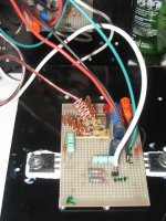
Well, the cooling fin idea ran into trouble, and had to be altered. I managed to cut the fins into shape OK, and even tinned the ends, after a fashion, but nothing I tried would get them to solder to the board. My only high-power soldering iron is a 120W monster with a tip the size of a pencil, so that wouldn't do, and my little 25W general-purpose one just wouldn't do the job.
So I changed tack, and made some heatsinks from 1.5mm copper wire, folded up into little concertina shapes. Each is about 10cm long stretched out, and one end soldered onto the right points on the board no problem. At least, five out of six did... doing the last one the SMD resistor adacent and both copper pads came off (My guess is that I weakened them messing around with the fins, but no way to be sure.) So a delicate repair job later, and all is well again. I have attached a picture of one channel with the heatsinks attached; my guess is that juma's idea would be more effective in general, but in this case the possible is better than the impossible. (And in any case, after an hour and a half they are barely warm to the touch, which suggests they are sufficient.)
Also this evening, I hooked the amp up to the main system in the living room to try to get a clearer idea of the sound. To give a little background, the system in my office is diy DAC followed by a commercial Creek (active) preamp, then the new amp and very ordinary speakers salvaged from an old mid-fi Aiwa system. (My diy FE127 speakers died due to a burned-out mosfet and my foolishness) The living room system is better - Airport Express receives data from the LAN, optically connected to a little made-in-China DAC, then to a diy B1 preamp, a diy F5 and B&W monitor speakers. Here's some preliminary findings, in no particular order.
1. The new amp is far better than the Hiraga Le Monstre it is replacing in the office. Really no comparison. It should be borne in mind that (both) the Monstre(s) was(were) made using nearest-modern-equivalent components, so this isn't a completely fair comparison, nonetheless there it is.
2. The new amp compares surprisingly well with the F5 - I expected the lower power to be more obvious, but not so. In fact, it appears to have more gain (crudely measured by looking at the volume control playing the same piece of music through each amp...) Possibly the F5 really needs something just a little stronger than the B1 (as juma mentioned in his thread on the BF862 preamp...) whereas this mini-aleph-j seems to pair well with the B1.
3. Female voice (Jessye Norman singing Strauss Lieder) sounded particularly good on the new amp on the living room setup - a slight warmth of tone compared to the F5. (Is it possible this is the famous "second harmonic glow"?) Whereas for piano music (Artur Pizarro playing the Apassionata) I think the F5 sounded marginally better. I listened to a little orchestral music which sounded good on both, but I would expect the extra power of F5 to give it the edge here if I listened for longer. As noted above, maybe I'll have to build the BF862 preamp to really see where this extra muscle counts.
Well, there you have it. Please bear in mind that these are only subjective opinions, but it seems better to post them than just to say " the amp sounds good...". I'll report more extensively when I've listened some more (and when initial enthusiasm has worn off, of course, which is a little fairer...)
Cheers
Nigel
So I changed tack, and made some heatsinks from 1.5mm copper wire, folded up into little concertina shapes. Each is about 10cm long stretched out, and one end soldered onto the right points on the board no problem. At least, five out of six did... doing the last one the SMD resistor adacent and both copper pads came off
(My guess is that I weakened them messing around with the fins, but no way to be sure.) So a delicate repair job later, and all is well again. I have attached a picture of one channel with the heatsinks attached; my guess is that juma's idea would be more effective in general, but in this case the possible is better than the impossible. (And in any case, after an hour and a half they are barely warm to the touch, which suggests they are sufficient.)Also this evening, I hooked the amp up to the main system in the living room to try to get a clearer idea of the sound. To give a little background, the system in my office is diy DAC followed by a commercial Creek (active) preamp, then the new amp and very ordinary speakers salvaged from an old mid-fi Aiwa system. (My diy FE127 speakers died due to a burned-out mosfet and my foolishness
) The living room system is better - Airport Express receives data from the LAN, optically connected to a little made-in-China DAC, then to a diy B1 preamp, a diy F5 and B&W monitor speakers. Here's some preliminary findings, in no particular order. 1. The new amp is far better than the Hiraga Le Monstre it is replacing in the office. Really no comparison. It should be borne in mind that (both) the Monstre(s) was(were) made using nearest-modern-equivalent components, so this isn't a completely fair comparison, nonetheless there it is.
2. The new amp compares surprisingly well with the F5 - I expected the lower power to be more obvious, but not so. In fact, it appears to have more gain (crudely measured by looking at the volume control playing the same piece of music through each amp...) Possibly the F5 really needs something just a little stronger than the B1 (as juma mentioned in his thread on the BF862 preamp...) whereas this mini-aleph-j seems to pair well with the B1.
3. Female voice (Jessye Norman singing Strauss Lieder) sounded particularly good on the new amp on the living room setup - a slight warmth of tone compared to the F5. (Is it possible this is the famous "second harmonic glow"?) Whereas for piano music (Artur Pizarro playing the Apassionata) I think the F5 sounded marginally better. I listened to a little orchestral music which sounded good on both, but I would expect the extra power of F5 to give it the edge here if I listened for longer. As noted above, maybe I'll have to build the BF862 preamp to really see where this extra muscle counts.
Well, there you have it. Please bear in mind that these are only subjective opinions, but it seems better to post them than just to say " the amp sounds good...". I'll report more extensively when I've listened some more (and when initial enthusiasm has worn off, of course, which is a little fairer...)
Cheers
Nigel
Attachments
Hi Nigel,
it's a great job you've done
I think you can get rid of the wire heatsink on Q4 - that JFET draws only 4-5mA (to supply the LED) so its' Pd can't be more than 85mW.
If it draws more than 5mA (measure the voltage across R13 to find out) increase the R13 up to 100R and readjust the DC offset after that.
- Status
- This old topic is closed. If you want to reopen this topic, contact a moderator using the "Report Post" button.
- Home
- Amplifiers
- Pass Labs
- Is a mini-Aleph using BF862 possible?