 amps. Otherwise they seem to be the same case..
chrismercurio said:I was thinking it might be economical to build the PS into a seperate enclosure and tap off of it Naim Style for the various Fx amplifiers.
What do you guys think? Is a possible, relevant, and viable option? More interested in the last 2 options as most things are possible.
/B]
Along similar lines ... I was going to attempt to build a 'universal First Watt' chassis. I.e. build up the +/- 24v power supply and have the ability to swap out various FW designs/boards (even allowing for some p2p wiring). I can populate boards relatively quickly, but chassis building, for me, is painfully slow. I think if one oversizes things enough e.g. heatsinks, transformers etc., it would be a nice test bed for these lovely amps. Just my two cents. I'm tired, of myself, for having populated boards sitting around unused.
... so many amps ... so little time
Ryan
chrismercurio said:I was thinking it might be economical to build the PS into a seperate enclosure and tap off of it Naim Style for the various Fx amplifiers.
What do you guys think? Is a possible, relevant, and viable option? More interested in the last 2 options as most things are possible.
The F amplifiers have commonalities - like Haiku.
1st rule: twin 18V secondaries

Re: Think current!
Maybe I'm wrong . . . but I have thought that, in this case, "all" feedback current will flow from the left to the right or opposite way through the feedback resistors and the cross bar, to generate feedback voltage at the Jffet Sources . . . And, here I'm assuming that the left and the right outputs will have the same voltage values of opposite polarities. This could be the reason why no X . . . On the course, the "very small error" (maybe ignorable) voltages must be shared by the both L/R Jfets tho . . .
Anyhow, it's interesting talk, isn't it?
zinsula said:In the F5, this current flows to ground, and here it flows to the other half of the circuit.
Maybe I'm wrong . . . but I have thought that, in this case, "all" feedback current will flow from the left to the right or opposite way through the feedback resistors and the cross bar, to generate feedback voltage at the Jffet Sources . . . And, here I'm assuming that the left and the right outputs will have the same voltage values of opposite polarities. This could be the reason why no X . . . On the course, the "very small error" (maybe ignorable) voltages must be shared by the both L/R Jfets tho . . .
Anyhow, it's interesting talk, isn't it?
Every afternoon I sit by the mailbox awaiting the current issue of AudioXpress...
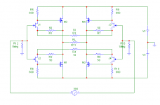
Just a quick sim -- this one tweaking the pots for minimum DC offset:
Just a quick sim -- this one tweaking the pots for minimum DC offset:
An externally hosted image should be here but it was not working when we last tested it.
Variac said:A minute ago I heard a magazine plop through my mail slot. Of course I leaped from my keyboard and down the stairs to find ..Stereophile ..
Attachments
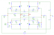
Re: Balanced F5
Ignore this schematic I resent the previous schematic by mistake.
I have attached the correct one.
Cheers
Tim
TimS said:I have simulated my previous balanced F5 and i got it to work after tweaking a few resistor values and reorienting some output devices (after my stupid mistake in the previous version of this schematic).
Ignore this schematic I resent the previous schematic by mistake.
I have attached the correct one.
Cheers
Tim
Attachments
Papa was quicker, doh.
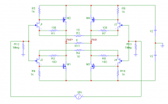
It won't work like this, biasing is via the 100R's, not the 10R's.
And to get the same voltage swing accross the load as with the straight and simple bridge, R4/R5 would be like 4 Ohms or so (and the other 4 all 10 Ohms). According to my quick sim, it gives x10 the distortion...
- Klaus
It won't work like this, biasing is via the 100R's, not the 10R's.
And to get the same voltage swing accross the load as with the straight and simple bridge, R4/R5 would be like 4 Ohms or so (and the other 4 all 10 Ohms). According to my quick sim, it gives x10 the distortion...
- Klaus
hehe
typical reactions of us , greedy boyz ;
Papa gave us new toy , now we want twice ......... or " double naked " , literally translated proverb from my native .......
anyway - I can't see easy X-ing that circuit , without resorting to good ole "out to gate " feedback scheme , and that way we are loosing virtues of low impedance feedback path .........
Papa certainly tried that iteration , so he can say is it worthwhile to x-it , or just plain bridging is best in this case ......
interesting dilemma .............
X , or low impedance feedback?
or - is it best to grab this bull between the horns ?
In reply How it currently works:
J1 is biased through R1. The offset that would be caused at Vout+ is cancelled by the equal current drawn by J2 and R2.
According to the simulation at 0V in J1 and J2 both draw about 3mA, this would in turn generate a 3V drop across R5, which in my simulation is enough to bias M2 to about 1A.
I think I see the Biasing error that Nelson is referring too, I should have source resistors on my mosfets to help stabilise the bias currents.
One of the nice advantages to this approach is that it has a common mode gain of 1 but a differential mode gain of (R1+R7)/R3
Nelson Pass said:A concept error
that happened to the bias
Who will first spot it?
Nelson has written
In traditional haiku
Five, seven, and five
Grey
- Home
- Amplifiers
- Pass Labs
- F5 power amplifier