Recently, I have been trying to put together a fun, simple project to make a headphone amplifier for use at the office. I plan to use this amplifier with a pair of Grado S80 headphones. I already have the PSU drawn up and the simulations look good for producing a smooth 20V through a standard LM317 voltage regulator. However, I wanted to check if my circuit looks correct because it is a modified version of the one from DIYaudioprojects.com found here: DIY IRF610 MOSFET Class-A Headphone Amplifier Project based on some suggestions I saw on this website. I guess my issue is when I run this simulation on LTSpice, it looks good until I get to the voltage being sent to the headphones themselves and I am not sure why or how I can verify this circuit. What kind of simulations should I be running? How can I switch this to reduce PSRR using a negative power supply or perhaps a P-Channel MOSFET? What alternative to the IRF610 would anybody suggest? I have so many questions.

Attachments
Last edited:
Why is there a 1Hz low-pass-filter in the gate drive? I think you've misdrawn this, the series 100k resistor is a big noise generator for instance.
That was from this post:
On the topic of the circuit originally suggested:
A Szekeres loaded with an LM317-based CCS at 250 mA, why not. As mentioned, it's clearly something for mains operation at half an amp of current draw (and requires adequate heatsinking if you do the math).
There are a few things I would definitely change about this one though. Here's the problems I spotted, which I think are fixable:
1. They specify a 10-20 V regulated supply partly because PSRR (power supply rejection) is not good. Assuming the bias pot is set to midpoint and a low-impedance source on the input, it's on the order of only 20 dB - that supply would have to be pretty darn clean indeed when you are planning to use typical 16 ohm earphones. That's the fault of the unfiltered input DC bias and highish source resistance.
2. Speaking of highish source impedance, I am not sure why that 4.7k series resistor is included at all, with a 150 ohm gate stopper already being present (which may or may not get the job done on its own, but would be easy to increase if needed). There is no filtering that would use it. Like this, its only function is to pointlessly increase high-frequency distortion (you want to drive MOSFETs with as low a source impedance as possible to minimize the effect of their parasitic capacitance), and reduce PSRR.
3. The pot for DC biasing is pretty quick'n'dirty breadboard DIY level and a more elaborate scheme would be advisable for the finished product. Adjustment range actually does not need to extend below Vgs,MOSFET + Vdrop,LM317 or about 4 V + 2 V ~= 6 V. As you can see, a 10 V supply would leave a maximum of about 4 V for Vdg, on 20 V it would be 14 V, which would reduce input capacitance nonlinearity quite a lot - or give room for much-improved level handling. (Best distortion for this kind of amp tends to be obtained when bias voltage is dialed down as far as voltage drop and signal peak amplitude will allow.) 20 V times 250 mA times 2 is 10 W, of course, plus power supply losses.
I therefore propose:
1. Remove 4.7k resistor and replace by direct connection
2. Remove the second 100k resistor (going to ground at 1 µF - pot wiper - 150R junction).
3. Between the pot wiper and 1 µF - 150R junction, add the following RCR filter components to clean up bias voltage:
* 100k series R
* about 10 µF (>= 25 V), going off to ground, polarity observing
* 100k series R
(one may have to go 2nd order but this should do)
4. Add a series resistor in the ground leg of the 100k adjustment pot. Depending on supply voltage to be used, this would range from about 150k @10V to 39k (43k) @20V. Compute as 100k * (6V / (V+ - 6 V)), with 6 V being the approximate minimum drop discussed above.
I would also use a bit more supply buffering than the single lonely 100n - current drawn is not, actually constant here (though relative variation would normally expected to be fairly small). Maybe an additional 22 µF per channel, and 470-1000 µF for both depending on your power supply.
Our RJM makes another sensible suggestion to further improve PSRR, namely having the MOSFET drain on the clean "ground" circuit node - even if that means you need a "Negative Nelly", err, negative voltage power supply if you want to stick with the n-channel MOSFET, otherwise you need a p-channel counterpart. Also observe the classic R/RC bias voltage filtering. I went for a slightly more complex variety because with a pot, filtering action would be heavily reduced or eliminated with the voltage turned all the way up.
To demonstrate the effect of this idea on PSRR, I re-reversed the "Reverso" (p-channel) version of the circuit, i.e. converted it from positive to negative supply so it's equivalent to a positive supply n-channel job. The result of both variations is attached. You can see that high-frequency PSRR is normally worsened by the effect of feedback capacitance (note the 1k input series resistor) when the FET drain is on the "dirty" power supply node. Towards the low frequencies we are also limited by maximum gain, being Av = gm * Rd = Id/Vt * Rd for a MOSFET amplifier. (An amplifier's gain makes a follower's PSRR.)
I am guessing there'll be more to be found on CCS-loaded Szekeres variations elsewhere.
in this thread Class-A Mosfet Headphone Amplifier where he suggest putting in an RCR filter to clean up the bias.
Also the gate bias isn't adjustable.
I was just doing that because I had not made the time to draw up a 100k potentiometer.
What would you suggest instead? This is my first amp build in a long time.
Last edited:
These buffer circuits don't give you any additional gain, which might be good to have for a headphone amp
If you are ok with a few more components this circuit i designed a long time ago works well
Sweet and Simple | Rock Grotto
A 10K log pot goes where the V2 voltage source is shown in the schematic
If you are ok with a few more components this circuit i designed a long time ago works well
Sweet and Simple | Rock Grotto
A 10K log pot goes where the V2 voltage source is shown in the schematic
Attachments
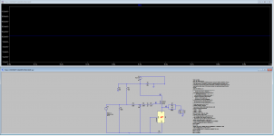
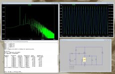
Fair enough. I will definitely have a look at making that one as well! Do you have a suggestion on log pots you like? Also, what am I doing wrong in my SPICE model for my circuit that my results look like this? Even if I make yours, I would like to understand more about the design I was attempting to put together as well as what simulations to look at.
Attachments
Where are you probing on those images?
It's helpful to add tags to key parts of the circuit - V_In, V_Out, VCC etc. Hit F4, add a label then place on the schematic.
Using node tags (not sure the right name) also helps clean the diagram - I place all voltage sources to one side and attach a VCC/VEE + GND node, then another on the appropriate point in the schematic.
At the very least, you misinterpreted what I wrote there. Connect C1 between R3 and R4 instead.
Be warned that LM317s may tend to oscillate if asked to drop more than about 8 V.
SR80s are reasonably sensitive; as such, unity gain should often be quite sufficient.
Can you tell me what you think of the circuit now? What about your implementation of improved PSRR? Do you have a .asc for that as well?
Thanks for the input.
Where are you probing on those images?
It's helpful to add tags to key parts of the circuit - V_In, V_Out, VCC etc. Hit F4, add a label then place on the schematic.
Using node tags (not sure the right name) also helps clean the diagram - I place all voltage sources to one side and attach a VCC/VEE + GND node, then another on the appropriate point in the schematic.
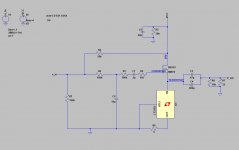
Updated the schematic. Now what are your thoughts?
Attachments
Updated the schematic. Now what are your thoughts?
I tend to keep the schematic as tidy as possible to make it easier to understand and navigate.
Like this:
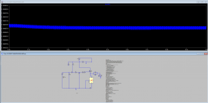
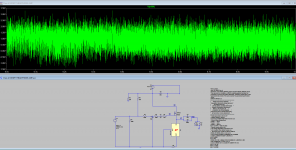
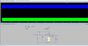
I've not looked at the circuit itself, but there is something wrong as it does not function when simulated.
Attachments
This is what i would do, if you were set on that design and its simplicity
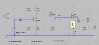
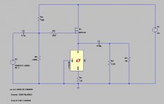
Can you tell me what my issue is now? I am going for simplicity, yes but I think I want to see if there are any minor tweaks that are worthwhile. Also, do you see any reason I would not want to implement the high pass filter to reduce noise in the DC bias seen here?
At the very least, you misinterpreted what I wrote there. Connect C1 between R3 and R4 instead.
Be warned that LM317s may tend to oscillate if asked to drop more than about 8 V.
SR80s are reasonably sensitive; as such, unity gain should often be quite sufficient.
But why not put the high pass before the DC bias is introduced to filter out low frequency noise at the point of input from the AC signal? As it has been a while since I got involved with analog circuits, I am just trying to understand as much as I can, so forgive the repetitive questions.\\
There's no DC bias at the FET's gate - C1 needs replacing with a wire. C2/R2 is a low-pass which will have a major impact on HF response, both R2 and C2 need substantial reductions in value. R3 I think should also be just a wire - its value can be rolled into R4 anyway.
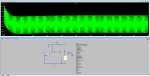
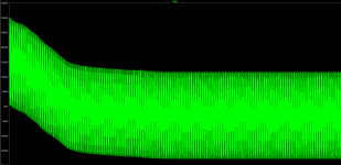
What values would you suggest? I went with one 50k resistor for this setup this time around, but still have issues with the output voltage as seen in my picture. I am missing something simple, I am sure.
View attachment Class A MOSFET HEADPHONE AMP LATEST VERSION.asc

Last edited:
To get going change C2 to something very small, try 22pF. The 50k also reduce, to 1k.
I downloaded your .asc and ran it. There's clearly something wrong with the IRF610 model, changing it for one of the FETs LTspice supports directly, I got sensible output and the LT317 biassed up correctly, taking 125mA.
I downloaded your .asc and ran it. There's clearly something wrong with the IRF610 model, changing it for one of the FETs LTspice supports directly, I got sensible output and the LT317 biassed up correctly, taking 125mA.
Can you tell me what my issue is now? I am going for simplicity, yes but I think I want to see if there are any minor tweaks that are worthwhile. Also, do you see any reason I would not want to implement the high pass filter to reduce noise in the DC bias seen here?
If you are filtering noise from the biasing voltage it is easier to do it at the power supply. Add a series resistor of a couple of ohms between VCC and C5/R5 and increase C5 to something like 2200uF.
To get going change C2 to something very small, try 22pF. The 50k also reduce, to 1k.
I downloaded your .asc and ran it. There's clearly something wrong with the IRF610 model, changing it for one of the FETs LTspice supports directly, I got sensible output and the LT317 biassed up correctly, taking 125mA.
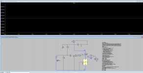
Changed the schematic according to your suggestions. I am still having the same problem even with the LT MOSFET though. Can you help me out?
If you are filtering noise from the biasing voltage it is easier to do it at the power supply. Add a series resistor of a couple of ohms between VCC and C5/R5 and increase C5 to something like 2200uF.
Done, but I am still not seeing a good output voltage at the headphones and I just don't see where I am going wrong.
I am attaching my PSU as well. I have a 12-0-12 2A transformer laying around I would really love to put to use, but LTSpice showing me some problems there.
I really appreciate all the help.
Attachments
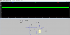
Changed the schematic according to your suggestions. I am still having the same problem even with the LT MOSFET though. Can you help me out?
I suggest you instantiate the FET with a specific part. I found IRF510 is present in my LTspice library, this gives a working circuit.
I suggest you instantiate the FET with a specific part. I found IRF510 is present in my LTspice library, this gives a working circuit.
That seemed to do the trick! Any ideas where I am going wrong with my PSU?
**PSU in next post**
Thanks.
Attachments
Last edited:
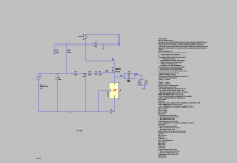
This is the PSU I keep having problems with. As I said, I want to use the 12-0-12 I have laying around here. It actually measures about 14-0-14 on my DMM (with no load).

Attachments

Last edited:
The error message I got says that your '12' labels need removing as labelling nets the same connects them together. After I removed both, the circuit worked - though the primary currents are very high as your transformer has an extremely low shunt inductance - suggest change it (and the secondaries in proportion) to 100H to be more realistic.
The error message I got says that your '12' labels need removing as labelling nets the same connects them together. After I removed both, the circuit worked - though the primary currents are very high as your transformer has an extremely low shunt inductance - suggest change it (and the secondaries in proportion) to 100H to be more realistic.
Everything seems to be in working order! Any other suggestions for small changes that could be improved in the design? I am particularly wondering about the grounding scheme for this.


Attachments
- Status
- This old topic is closed. If you want to reopen this topic, contact a moderator using the "Report Post" button.
- Home
- Amplifiers
- Headphone Systems
- IRF610 Class A Headphone Amp