"The Crocodile" headamp
It is started a while ago, more like a joke. Attempt to show that with a pretty simplistic nested feedback loop concept and a bunch of NE5532 it is possible to achieve a 0.1ppm distortion level for 20kHz signal at 33Ohm load and couple of Vrms. I sort of achieved the goal, with an exception of a few "but". Of course one of those "but" was, as almost any early stage proto, it looked ugly as hell:

Long story short, I managed to squeezed it into a 50x50mm PCB (sorry, no imperial units allowed!) to get PCBs for cheap from the Seedstudio. So, here it is. It is green, it is still somewhat ugly, and someone called it "a crocodile", so I decided - Crocodile it is")

Although I didn't stick with 5532 this time. Tried some different opamp, to see how it goes.
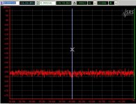
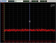
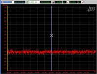
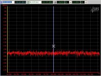
There are some measurement results on a 33Ohm load. In case of the 20kHz signal, the output amplitude is 4VRms (+12dBVrms), for the IMD test it is mixture of two 2Vrms (+6dBVrms) signals.
It is not hard to make something better using the same number of opamps, but the moto was "as straightforward as possible"
It is started a while ago, more like a joke. Attempt to show that with a pretty simplistic nested feedback loop concept and a bunch of NE5532 it is possible to achieve a 0.1ppm distortion level for 20kHz signal at 33Ohm load and couple of Vrms. I sort of achieved the goal, with an exception of a few "but". Of course one of those "but" was, as almost any early stage proto, it looked ugly as hell:
Long story short, I managed to squeezed it into a 50x50mm PCB (sorry, no imperial units allowed!) to get PCBs for cheap from the Seedstudio. So, here it is. It is green, it is still somewhat ugly, and someone called it "a crocodile", so I decided - Crocodile it is
Although I didn't stick with 5532 this time. Tried some different opamp, to see how it goes.
There are some measurement results on a 33Ohm load. In case of the 20kHz signal, the output amplitude is 4VRms (+12dBVrms), for the IMD test it is mixture of two 2Vrms (+6dBVrms) signals.
It is not hard to make something better using the same number of opamps, but the moto was "as straightforward as possible"
Attachments
Last edited:
Here is the schematic.
Sergey888: A good looking design! I'm just now getting a chance to circle back and have a look.
Am I right that in your notation R51_C2 would be R51 for channel 2? At first I was thinking that was some sort of RC combination!
I see you have added 2.2R's to the feed back loops of the buffers to cancel the drop caused by R65. I wanted to do that on the O2 booster board, but NwAvGuy's equivalent of R65 is 40.2K. I figured that would add too much noise if I put one in each buffer feedback loop. But for just 2.2R in your case that works great.
Also, should those buffer feedback resistors (R50, 52, 66, 67) be 2.2R * 4 = 8.8R? I was pondering that once with the booster board. Since the DC current through R65 would be the sum of all four buffer input bias currents, the R65 voltage drop would be 4x that caused by any one buffer's bias current. It seems like the cancelling resistors would have to be 4x since they only see 1x the bias current.
I see you used your 2nd order feedback network on the 1611! And you wrapped the buffers around with global feedback via R53 and R56. So here is a question about stability.
The bandwidth and the slew rate of the 1611 are both considerably greater than that of the NE5532 buffers. When I tried that with the NJM4556A chips as a test in an early ODA design it oscillated, no matter what I did. I could see on the scope that the slow NJM4556As just could not keep up with the higher slew rate of the chip I had looped around driving them. I would get square waves on the output as the slow buffer chip did its best to keep up with the faster input slewing. How did you solve that faster-feeding-slower problem? I'm guessing that you have slowed down the 1611 in a way that I haven't figured out yet.
Last edited:
Hey!
Let me try to answer.
Yep. I have used a hierarchical design with two identical blocks (C1, C2) for two channels. Altium automatically adds this suffix to the reference designators.
R50...R67 - these are just place holders. They are added to allow using of CFA instead, putting some appropriate value resistors. They suppose to be just a 0 Ohm links. 2.2 Ohms value is used because it is already present in the schematic, to keep values count lower. R65 of 22Ohm is to low to creature a significant offset. And it will be compensated in the loop anyway, even if it was significant.
C69 C70 R61 are not actually used. Placeholders again. Just in case if someone wants to try different variants. I decided to save a few values and compensated it only with C64 R55.
In this case output opamp higher slew rate. I've used LM6172. The oscillations you have seen may be not only because of slew rate difference. Depends on the amplifier structure.
Last edited:
OK, I see now. Well congratulations on the measured results! Pretty impressive. It looks like you have a switcher on there for the power supply and none of that (switching frequency) seems to be making it into the audio.
Input lead-lag compensation? And am I looking at it right that the stage is inverting?
Now I understand (on stablity)! 3000V/uS and 100MHz bandwidth it looks like, for the 6172. Right up there with the LME49600, just 50mA vs. the 250, and it is a complete unity-gain stable op amp rather than just a buffer. I just skimmed through the datasheet. I see that rather than a THD number they are listing the 2nd and 3rd harmonics. Those should be the biggest contributors anyway. Interesting! Another ADSL driver, like the TPA6120's earlier incarnation.
That inductor bypassed output resistor to isolate the load capacitance (L50 and R64) is a good idea. I know jcx has posted about using something similar before on this TPA6120 designs. Are you actually using the R62/C71 Zobel-looking network on each side, or are those placeholders too?
It looks like you have a switcher on there for the power supply and none of that (switching frequency) seems to be making it into the audio. I decided to save a few values and compensated it only with C64 R55.
Input lead-lag compensation? And am I looking at it right that the stage is inverting?
In this case output opamp higher slew rate. I've used LM6172. The oscillations you have seen may be not only because of slew rate difference. Depends on the amplifier structure.
Now I understand (on stablity)!
3000V/uS and 100MHz bandwidth it looks like, for the 6172. Right up there with the LME49600, just 50mA vs. the 250, and it is a complete unity-gain stable op amp rather than just a buffer. I just skimmed through the datasheet. I see that rather than a THD number they are listing the 2nd and 3rd harmonics. Those should be the biggest contributors anyway. Interesting! Another ADSL driver, like the TPA6120's earlier incarnation.That inductor bypassed output resistor to isolate the load capacitance (L50 and R64) is a good idea. I know jcx has posted about using something similar before on this TPA6120 designs. Are you actually using the R62/C71 Zobel-looking network on each side, or are those placeholders too?
Last edited:
It looks like you have a switcher on there for the power supply and none of that (switching frequency) seems to be making it into the audio.
It is not too hard to filter out SMPS frequency.
Input lead-lag compensation? And am I looking at it right that the stage is inverting?
Yeah, more like lag than a lead
It is easy to convert it into non-inverting, with a few wire links and a couple of extra passives.Another ADSL driver, like the TPA6120's earlier incarnation.
It is not a CFA though.
That inductor bypassed output resistor to isolate the load capacitance (L50 and R64) is a good idea. I know jcx has posted about using something similar before on this TPA6120 designs. Are you actually using the R62/C71 Zobel-looking network on each side, or are those placeholders too?
Yep, I use them all. It is a little bit better for damping possible resonances. Like driver inductance - cable capacitance etc. Potentially it can be simplified without too much harm, but it is just a two more passives.
Sergey888 - so another question for you.
The four LM6172s at 50mA each should total up to around 200mA, minus balancing DC currents. Since they are duals that would be 2 SOIC8 packages. Would you expect your results here to outpeform the same circuit with one 250mA LME49600 in place of the four LM6172s or would you expect the results to be more or less similar? The LM6172s certainly have less inherent THD it seems from the datasheet, but with looped gain + buffers like this is seems like the results are mostly influenced by the driving chip. I'm curious how much the buffer's specs actually matter.
Also question on your board... so am I right that you have both channels on the one board, but have just built up one channel for testing? I'm guessing those two blank pads on the left side would be the LM6172s for the other channel. What are the dimensions of your board? You probably have just beaten the O2 headamp. NwAvGuy used just the one dual output chip (70mA per opamp NJM4556A) in parallel on each channel, which has proved to not have enough power dissipation at 16R load with low sensitivity cans and high volume levels (chips crack in half). His design also overheats the output chips with +/-15V rails with a 32R load. But since you have double the output chips on each channel with twice the dissipation (minus some for surface mount vs. DIP) yours would probably go further. Have you worked out what the maximum Vrms output swing would be into 32R to keep the output chip dissipation within limits?
Plus you managed to get a switcher on it! The O2's (linear, and not heat sinked) voltage regulators tend to get nuclear-hot with higher output loads and/or more than 12Vac in. No such problem with the switcher.
The four LM6172s at 50mA each should total up to around 200mA, minus balancing DC currents. Since they are duals that would be 2 SOIC8 packages. Would you expect your results here to outpeform the same circuit with one 250mA LME49600 in place of the four LM6172s or would you expect the results to be more or less similar? The LM6172s certainly have less inherent THD it seems from the datasheet, but with looped gain + buffers like this is seems like the results are mostly influenced by the driving chip. I'm curious how much the buffer's specs actually matter.
Also question on your board... so am I right that you have both channels on the one board, but have just built up one channel for testing? I'm guessing those two blank pads on the left side would be the LM6172s for the other channel. What are the dimensions of your board? You probably have just beaten the O2 headamp.
NwAvGuy used just the one dual output chip (70mA per opamp NJM4556A) in parallel on each channel, which has proved to not have enough power dissipation at 16R load with low sensitivity cans and high volume levels (chips crack in half). His design also overheats the output chips with +/-15V rails with a 32R load. But since you have double the output chips on each channel with twice the dissipation (minus some for surface mount vs. DIP) yours would probably go further. Have you worked out what the maximum Vrms output swing would be into 32R to keep the output chip dissipation within limits?Plus you managed to get a switcher on it! The O2's (linear, and not heat sinked) voltage regulators tend to get nuclear-hot with higher output loads and/or more than 12Vac in. No such problem with the switcher.
Last edited:
The four LM6172s at 50mA each should total up to around 200mA, minus balancing DC currents. Since they are duals that would be 2 SOIC8 packages. Would you expect your results here to outpeform the same circuit with one 250mA LME49600 in place of the four LM6172s or would you expect the results to be more or less similar? The LM6172s certainly have less inherent THD it seems from the datasheet, but with looped gain + buffers like this is seems like the results are mostly influenced by the driving chip. I'm curious how much the buffer's specs actually matter.
Buffer distortions will be suppressed by the gain depth the first opamp has at a particular frequency in a particular gain configuration. The lower GBW opamp you use, the more it matters.
You can estimate the worst possible case distortion for LM6172 for my case, assuming that it all comes from the LM's side. For example OPA has around 63dB gain @ 60kHz, minus 6dB for the noise gain, so there is around 57dB of the loop gain left. It means that LM's 3rd harmonic is at least 83dB down.
Also question on your board... so am I right that you have both channels on the one board, but have just built up one channel for testing? I'm guessing those two blank pads on the left side would be the LM6172s for the other channel. What are the dimensions of your board?
Yep, there are two channels on the PCB. You can see it from the schematic too.
It is 50x50mm. Was the aim to fit into Seeedstudio's smaller PCB size to get a good price.
You probably have just beaten the O2 headamp.
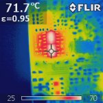
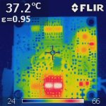
I run it on +/9V. Hard to tell what it would be inside a box. Can have a look with an infrared camera what is going on while it is on the bench.
Plus you managed to get a switcher on it! The O2's (linear, and not heat sinked) voltage regulators tend to get nuclear-hot with higher output loads and/or more than 12Vac in. No such problem with the switcher.
You can also make a switch to change the supply voltage, for a high and low impedance loads.
Last edited:
adydula - you should consider building one! Sergey888 is one of the folks on the forum that I have a lot of technical respect for. Several of his suggestions went into the O2 booster board.
I'm just asuuming Sergey888 doesn't have any build instructions written up but should be able to figure it out from the schematic and a few posts as needed. Those buffer chips he is using are really interesting. Take a look at their datasheet! I think he mentioned those during the design of the O2 booster board but I wanted to stick with the LME49600s for that one. Plus he has measured the results!
I'm probably going to send an order off to Arrow next week for some stuff. I see they have the LM6172 for just $2.99 each, so the four would clock in at $12, plus the two OPA1611 for $3.25 each and the LT3467 switcher which is $3. Saves a bunch of money over Mouser, at least if you have an order big enough to cover their shipping. I'll have to check on the LT chip though. They show minimimum order quantity 1, but then only show the price for 10.
Sergey888 - interesting about the thermal scan! So all the heat that isn't dissipated by the package body goes out via the chip leads to the foil?
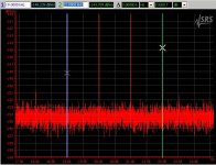
Also just curious - I see the SRS logo on your plots. Are you using a SR1? Those look like nice units.
Sergey888 is one of the folks on the forum that I have a lot of technical respect for. Several of his suggestions went into the O2 booster board.I'm just asuuming Sergey888 doesn't have any build instructions written up but should be able to figure it out from the schematic and a few posts as needed. Those buffer chips he is using are really interesting. Take a look at their datasheet! I think he mentioned those during the design of the O2 booster board but I wanted to stick with the LME49600s for that one. Plus he has measured the results!
I'm probably going to send an order off to Arrow next week for some stuff. I see they have the LM6172 for just $2.99 each, so the four would clock in at $12, plus the two OPA1611 for $3.25 each and the LT3467 switcher which is $3. Saves a bunch of money over Mouser, at least if you have an order big enough to cover their shipping. I'll have to check on the LT chip though. They show minimimum order quantity 1, but then only show the price for 10.
Sergey888 - interesting about the thermal scan! So all the heat that isn't dissipated by the package body goes out via the chip leads to the foil?
Also just curious - I see the SRS logo on your plots. Are you using a SR1? Those look like nice units.
Last edited:
I'll try to make a simple assembly drawing soon. Should make things easier.
LT part potentially can be replaced with some NS parts, like LM2733, LM27313, LMR64010
etc. Also I don't know if they will be stable in this configuration (most likelly they will, but who knows) and what output noise density at low freq end will be. LT one turns out to be rather quiet one. It's not as critical but nice to have.
Yeah, it is quite like that for small packages. Thicker copper really helps. More layer or a thinner PCB will also improve dissipation, if you have internal or opposite side planes.
Yes, it is SR1. Nice thing.
Last edited:
ok how can I get aboard?
Alex
Shoot Sergey888 a PM. He already has mine in the mail!
Sergey888 - are there any parts on the other side of the board other than the terminal strips? Please post a photo of the other side if you get a chance.
- Status
- This old topic is closed. If you want to reopen this topic, contact a moderator using the "Report Post" button.
- Home
- Amplifiers
- Headphone Systems
- "The Crocodile"