Yes, it's in post #36. http://www.diyaudio.com/forums/digital-source/254063-ad1862-pcb-layout-4.html#post3891624
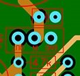
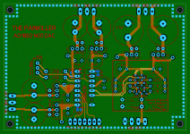
Firstly, if your PCB layout program has a DRC (design rules check) function I would recommend that you learn how to use it. The first picture shows a trace running very near a GND pin, if this does not cause a short during PCB manufacture, it will probably short when you solder that GND pin.
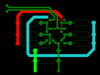
The 2 resistors, the connector in the RH edge next to the text PAINKILLER can be moved so the tracks to the IC are short (rotate the resistors) and place the connector accordingly (don't rotate) this will minimise the digital signals loop area greatly.
Finally with this quick look, the output section is a bit scrappy in terms of connections going everywhere, again this is low level analogue output reducing the loop area of these signals and making them as small as possible is advantages, it is better to make the power routes a bit longer and minimise the signal lengths. A possible solution is shown in the second picture. When laying out a board these days signal lengths and loop areas take precedence over component placement looking pretty (i.e. all lined the same way in nice lines, that went out of the window many years ago as maximising signal integrity and EMC protection is the critical function of a layout).
")
Woops pictures have loaded wrong way round!
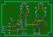
The red and blue traces are the +/- 18V routed on the bottom layer (as are the two red traces).
The 2 resistors, the connector in the RH edge next to the text PAINKILLER can be moved so the tracks to the IC are short (rotate the resistors) and place the connector accordingly (don't rotate) this will minimise the digital signals loop area greatly.
Finally with this quick look, the output section is a bit scrappy in terms of connections going everywhere, again this is low level analogue output reducing the loop area of these signals and making them as small as possible is advantages, it is better to make the power routes a bit longer and minimise the signal lengths. A possible solution is shown in the second picture. When laying out a board these days signal lengths and loop areas take precedence over component placement looking pretty (i.e. all lined the same way in nice lines, that went out of the window many years ago as maximising signal integrity and EMC protection is the critical function of a layout).
Woops pictures have loaded wrong way round!
The red and blue traces are the +/- 18V routed on the bottom layer (as are the two red traces).
Attachments
Last edited:
Drill sizes, the general rule of thumb for plated through holes is lead diameter plus 0.2mm.
For non-plated through holes lead diameter plus 0.1mm; you want a tighter fit to give as much mechanical help to a single sided solder joint as they are more prone to movement of the component due to vibration or thermal stress. Whereas a PTH joint has its strength in the solder joint up the barrel of the plated hole.
For non-plated through holes lead diameter plus 0.1mm; you want a tighter fit to give as much mechanical help to a single sided solder joint as they are more prone to movement of the component due to vibration or thermal stress. Whereas a PTH joint has its strength in the solder joint up the barrel of the plated hole.
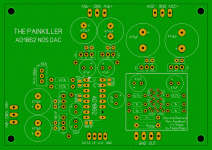
Thanks! That is good feedback. Your layout for the transistors is definitely better. Tried to follow your suggestion, but with some small modification. Does it look ok now?
Moved the MSB-trim. Maybe using SMD-resistors would be better, in order to minimize the loop?
I also created some thermal relief for the gnd pads, and checked all hole sizes.
Moved the MSB-trim. Maybe using SMD-resistors would be better, in order to minimize the loop?
I also created some thermal relief for the gnd pads, and checked all hole sizes.

Hi Painkiller, Hi Marce,
sorry for my two cents question here, my understanding of pcbs is very low :
Marce I read the didactics links you gave in recent threads.
on the last first picture : we have two leads (current output signal?) going through between two pin of a cap. Could it be better to avoid it and run below the pins of the cap as there is space free ?
idem on the pedja circuit : could it be better then the two leads run below the last resistor bench 1K ((little space for oblic leads between the 1K & the Riv horizontal resistor) to avoid leads crossing or is it not a problem ?
When no space free, could it be better to ending a lead with a trough all to jump with a good wire (with gnd or not ,) to avoid crossing two others leads (but permitt this crossing with more space to avoid coupling like we saw in the 80s' sometimes with commercial products ? (for DIY I mean when no 4 layers pcb possibility)
For the I2S ? No GSGSGSG throughs holes or UFL connection connectors... maybe because molex connection ?
sorry if it seems a stupid question...
sorry for my two cents question here, my understanding of pcbs is very low
:Marce I read the didactics links you gave in recent threads
.on the last first picture : we have two leads (current output signal?) going through between two pin of a cap. Could it be better to avoid it and run below the pins of the cap as there is space free ?
idem on the pedja circuit : could it be better then the two leads run below the last resistor bench 1K ((little space for oblic leads between the 1K & the Riv horizontal resistor) to avoid leads crossing or is it not a problem ?
When no space free, could it be better to ending a lead with a trough all to jump with a good wire (with gnd or not ,) to avoid crossing two others leads (but permitt this crossing with more space to avoid coupling like we saw in the 80s' sometimes with commercial products ? (for DIY I mean when no 4 layers pcb possibility)
For the I2S ? No GSGSGSG throughs holes or UFL connection connectors... maybe because molex connection ?
sorry if it seems a stupid question...
Last edited:
I haven't had a good look at the design yet as I've just got to my hotel.
Eldam, I agree about the leads through the cap, plenty of room...so I would agree that the cap can either rotate 180 deg or move the traces down.
I'll look at the rest later, 5 hours of painful UK train travel, I am now going to drink lots of bear and hammer room service
The more people that do look at a layout the better, that way you are more likely to get a thorough check as each person will look at it a different way and spot different things.
Cheers now its...

agree with last point more on that later...
Eldam, I agree about the leads through the cap, plenty of room...so I would agree that the cap can either rotate 180 deg or move the traces down.
I'll look at the rest later, 5 hours of painful UK train travel, I am now going to drink lots of bear and hammer room service
The more people that do look at a layout the better, that way you are more likely to get a thorough check as each person will look at it a different way and spot different things.
Cheers now its...
agree with last point more on that later...
Agree Marce, that's I try to explain to some people (in the thread i talked to you) about "the more people!" happy to see that just my 2 cents input can be good enough if goodwilled !
Pffff you move a lot ! GB needs frencch fast trains... it seems there are more and more active towns in Britains... Have a good rest.
Pffff you move a lot ! GB needs frencch fast trains... it seems there are more and more active towns in Britains... Have a good rest.
I think I could move the cap a bit upwards, without making the loop to ground any longer, and then run the traces around the cap. Is it a problem with the signal trace crossing the -18V line?
About the I2S input. I don't know what's the right configuration. Is there some sort of standard for this? Is there really need for 4 ground connections? I've made the pads for a regular 2,54 mm pitch terminal block. I don't want UFL connectors. The UFL cables are costly, tend to break easily and only come in standard lengths. I'd rather run shorter lengths of regular cable.
All feedback is welcome. The more the merrier! I'm very thankful for all the input I've been getting on this design. Hope it will turn out ok in the end.
About the I2S input. I don't know what's the right configuration. Is there some sort of standard for this? Is there really need for 4 ground connections? I've made the pads for a regular 2,54 mm pitch terminal block. I don't want UFL connectors. The UFL cables are costly, tend to break easily and only come in standard lengths. I'd rather run shorter lengths of regular cable.
All feedback is welcome. The more the merrier!
I'm very thankful for all the input I've been getting on this design. Hope it will turn out ok in the end.Hi painkiller,
Don't know for the - 18 v... and I don't understand if the data current line are on the same side than the the - 18 anf if not if the thickness of the pcb avoid problems if here the leads cross the one beneath at 90° like you draw (for me PS & Digital or analogic leads should not be crossed if no continous gnd between (multilayers ground plane)....but I'm not sure, I'm a perpetual student in Audio )
GSGSGS(G) : G holes are here to allow flat cable with the return Gnd near the signals... it's RF ! (IF NOT COAXIAL with the U.FL plugs and wires you want to avoid !
My understanding is the longer of I2S sould not be more than 10 cm chip to chip not to creat more problem than solving one?! Maybe for lower frequencies you can go for bigger length ? here it's not 50 MHz ! I don't know but I read often : less than 10 cm !
But if you have the Ian Fifo does it no tuse any U.FL connectors and wires ?
Don't know for the - 18 v... and I don't understand if the data current line are on the same side than the the - 18 anf if not if the thickness of the pcb avoid problems if here the leads cross the one beneath at 90° like you draw (for me PS & Digital or analogic leads should not be crossed if no continous gnd between (multilayers ground plane)....but I'm not sure, I'm a perpetual student in Audio
)GSGSGS(G) : G holes are here to allow flat cable with the return Gnd near the signals... it's RF ! (IF NOT COAXIAL with the U.FL plugs and wires you want to avoid !
My understanding is the longer of I2S sould not be more than 10 cm chip to chip not to creat more problem than solving one?! Maybe for lower frequencies you can go for bigger length ? here it's not 50 MHz ! I don't know but I read often : less than 10 cm !
But if you have the Ian Fifo does it no tuse any U.FL connectors and wires ?
The -18V trace and the analog signal between dac and IV are crossing on adjacent layers with no ground plane in between. I don't know if this is something that should be avoided or not.
The iancanada I2S converter only uses U.FL for mck input. The output has a GSGSGSGSG configuration. So perhaps I should use a similar input on the dac board. The idea is to minimize the cable length here. Down towards 2 cm.
The iancanada I2S converter only uses U.FL for mck input. The output has a GSGSGSGSG configuration. So perhaps I should use a similar input on the dac board. The idea is to minimize the cable length here. Down towards 2 cm.
I2S-PCM output is different then what you've wrote - see attached....The iancanada I2S converter only uses U.FL for mck input. The output has a GSGSGSGSG configuration. So perhaps I should use a similar input on the dac board. The idea is to minimize the cable length here. Down towards 2 cm.
Attachments
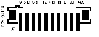
I2S-PCM output is different then what you've wrote - see attached.
Yup, I stand corrected.
I guess the correct input should be GND-DATA-GND-LE-GND-CLK-GND. That way all the gnd pins from the I2S-PCM would be used, but only one data line for each board.
Hé I will ask you to sell me one board when it will be finish... looks good, and it's the best 20 bits chip ever maid for me !
I don't know if it's important but this is exactly how I expect the signal leads to be !
i you make 45 trigonometric rotation with the 47 uf cap, the lead will be two time shorter & theorical better decoupling. I think Marce would say : put before the trough hole and the dac pin a smd trace to gnd for a 100 nf SMD X7R/COG cap for the pin decoupling. But If you want to stay with your ratio with decoupling 1 to 10... or 1 to 47 : try a 1210 case leads for Cornell Dublier acrylic (1 uF max)...but marce will fight me and will say X7R 100 nf 603 case or 405 if you hand are able to !)
If i understood you : if you make a mirror of this design in a unique pcb, you have noise on one of the channel ?
Yes, I'll check with Pedja. Hopefully he'll be ok with me sharing his circuit design.
The signal leads are now a bit longer, but they're also shielded from the psu lines by a ground plane. Perhaps this is better.
Good idea rotating the cap a bit. The 47uF and 4.7uF caps are filter caps for the internal voltage reference. The datasheet recommends 1uF and 10uF or larger, and always a 1:10 ratio. I don't know if 100nF smd caps are necessary here, or if they are even recommended. If I reduced them to 22uF and 2.2uF the cap would use up less space and the loop to ground would be shorter. But I'm not sure about parallel smd caps in this position. As for the psu decoupling there are 100nF x7r 0805 caps on all rails.
This is a mono dac board. Placing two chips on one board would result in mixing up the analog and digital grounds. When I tried this on a prototype board one channel was always noisy. Stacking mono boards on top of each other is a better solution.
- Home
- Source & Line
- Digital Line Level
- AD1862 PCB layout