Hi all,
For those who like to build DAC circuits rather than to apply DAC chips:
While I was working on my valve DAC I got curious about how well a conceptually similar circuit built with CMOS logic gates and active filters could work. Using 74AHC02 and 74AHC08 CMOS logic gates as the DAC (a four-tap return-to-zero FIRDAC) with a very straightforward crystal oscillator and an LT3042 voltage reference, I measured a noise floor of about -97 dB(A) with respect to the maximum signal level. The schematics are attached, the FPGA code is the same as the FPGA code for my valve DAC that can be found on the Linear Audio website.
The FPGA code contains a sigma-delta modulator that has three modes: seventh-order chaotic and two fifth-order modes with embedded pulse width modulator. In the valve DAC the PWM8 mode clearly has the smallest in-band noise, but with the 74AHC02/74AHC08 circuit it hardly makes any difference. The in-band noise floors are nearly the same for all modes:
PWM4: -97.83 dB(A)
chaos: -97.06 dB(A)
PWM4 (repeated measurement): -97.44 dB(A)
PWM8: -98.32 dB(A)
The out of band noise is different, as expected:
chaos: about 1.3 mV RMS
PWM4: about 2 mV RMS
PWM8: about 6.7 mV RMS
The out-of-band values are estimated by looking at the quasi peak-peak noise with an oscilloscope and assuming that the RMS value is about a sixth of the quasi peak-peak value.
The maximum signal level is about 1.96 V RMS. All values are differential voltages, the single-ended voltages are half the differential voltages.
Best regards,
Marcel van de Gevel
Edit, 30 May 2023:
Hans Polak has done measurements and experiments and among many other things, found that the noise floor is substantially lower than I measured, see https://www.diyaudio.com/community/...ith-97-db-a-dynamic-range.313520/post-7363723
Attachments
Last edited:
Hi all,
The schematics are attached, the FPGA code is the same as the FPGA code for my valve DAC that can be found on the Linear Audio website.
Best regards,
Marcel van de Gevel
Great and very interesting project.
Could you please post the FPGA code also here to me and others also interested?
Thank you in advance,
Ronaldo
Only partly; I've attached the Verilog and filter coefficient files, a constraint file and a text file with settings, but a pdf file about how to generate the FIR filters and FIFOs is not included because of file size limits.The same holds for an MCS file that you could directly put into the configuration memory without synthesizing anything. For these files, please see Downloads | Linear Audio
Actually the delay until the output relay is energised is too short for the circuit in this thread, so there is a power-on thump. I should change that and re-synthesise the whole thing.
By the way, the FPGA module has R102 mounted and R103 not, which means that IO bank 0 runs on 3.3 V (see http://www.trenz-electronic.de/file.../TE0630_series/TE0630/documents/UM-TE0630.pdf ).
Attachments
Last edited:
Each CMOS logic gate drives a 32K4 resistor; the output resistance of the gate is in series with 32K4. The 74AHC08 datasheet guarantees that its output resistance will be lower than (0.36V / 8mA) = 45 ohms; probably half of that on a typical unit.
I'm wondering, how important is this effect? What fraction of "1 LSB" does it represent?
I'm wondering, how important is this effect? What fraction of "1 LSB" does it represent?
Attachments
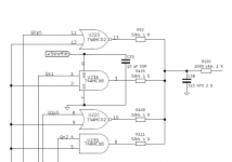
Each CMOS logic gate drives a 32K4 resistor; the output resistance of the gate is in series with 32K4. The 74AHC08 datasheet guarantees that its output resistance will be lower than (0.36V / 8mA) = 45 ohms; probably half of that on a typical unit.
I'm wondering, how important is this effect? What fraction of "1 LSB" does it represent?
What is important using CMOS for these kinds of uses is not so much the output impedance but the symmetry for high vs low output levels. In my experience this is better than even a 10% mismatch. That is where the complimentary process is so important. As shown I would expect to see 14 bits of accuracy from a single output.
Actually differences between the output resistances for high and low levels are the reason why I chose a balanced structure. These resistance differences now mainly cause a common-mode error, because for every high output there is a low output on the other side.
If there were no difference at all between the output resistances for high and low levels, the output resistance would simply add to the 32.4 kohm and would only affect the filter characteristic a bit.
(For the record, the filter resistors I use are mostly 0.5 % tolerance thin film SMD resistors and most of the NP0 capacitors have 1 % rather than the specified 2 % tolerance.)
Last edited:
The problem with unequal resistances for high and low levels (particularly in the unbalanced case) is that it makes the low-pass filter time variant. A time-variant filter can convert out-of-band quantization noise into the audio band. It is difficult to say anything quantitative about how bad this effect is.
Have you considered noise cancelling parts from Potato Semiconductor / The GHz TTL/ CMOS IO Interface Logic/ Potato IC ?
The problem with unequal resistances for high and low levels (particularly in the unbalanced case) is that it makes the low-pass filter time variant. A time-variant filter can convert out-of-band quantization noise into the audio band. It is difficult to say anything quantitative about how bad this effect is.
Are the 0.5% 32K4 resistor variations (leg #3_true is +162 ohms, leg #3_complement is -162 ohms) less troublesome, because they are constant whether the data bit is a high or a low?
Have you considered noise cancelling parts from Potato Semiconductor / The GHz TTL/ CMOS IO Interface Logic/ Potato IC ?
No, mainly because I didn't know they existed. Anyway, the exact waveforms shouldn't matter much with a return-to-zero design as long as everything settles properly well within half a clock cycle - or at least that's the theory, maybe there is some second-order effect why they matter after all.
Are the 0.5% 32K4 resistor variations (leg #3_true is +162 ohms, leg #3_complement is -162 ohms) less troublesome, because they are constant whether the data bit is a high or a low?
That's indeed what I would expect. As long as the filter remains linear and time invariant, it is not capable of converting out-of-band noise into the audio band, and I don't see how resistor tolerances could make it non-linear or time variant.
How many OSR did you use for DSM? I usually use 64(2.8MHz) or 128(5.6MHz) because more than 256 has less SNR. High OSR is the trade-off between less SNR and easy LPF for quantization noise as far as I have experienced. The latest DSM has better quality than older one such as SACD. Even 64 is adequate to eliminate quantization noise by simple 12dB/oct RC filter.
Hi xx3stksm,
That depends... I use a bit rate of 27 Mbit/s. In the chaotic mode the quantizer also runs at 27 MHz, in PWM4 mode at 6.75 MHz and in PWM8 mode at 3.375 MHz. What oversampling ratio that corresponds to by definition also depends on the sample rate of the source.
I can imagine that the error you get due to unequal rise and fall times in non-return-to-zero DACs increases with the clock frequency - after all, the transition time difference becomes a bigger percentage of the clock period. That issue should be solved in a return-to-zero DAC, but you can still get problems due to incomplete settling or due to jitter.
The bandwidth of my analogue reconstruction filter is about 85 kHz. I wanted to be able to reproduce most of the signal information in 192 kHz sample rate material and to have a bandwidth suitable for humans as well as domestic cats.
I made the order of the filter a bit higher than the order of the noise shaping, hoping that the spectral density of the noise would drop rather than increase above the band of interest, but that may not be a good argument. Right above the highest notch of the noise transfer function the noise always increases faster than with order*20 dB/decade and when the poles of the NTF kick in, the noise levels off anyway.
What reconstruction filter bandwidth and sigma-delta order do you use and how much out-of-band noise do you measure at the output of your second-order filter?
Hi MarcelvdG,
Honestly speaking, I can understand the advantage of FIR DAC like Signalist but can't understand those of RNZ. I can make my new PCB with a discrete DSM DAC by the end of next month. Then, I will examine the advantage of NRZ. A real PCB is always a good guru who gives me much advice.🙂
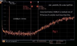
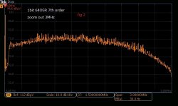
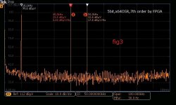
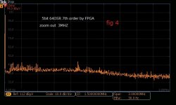
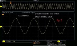
My first choice is, as I wrote before, multi-bit DSM rather than 1bit.The analog post filter is also intended for multi-bit DSM(5 bit).I finally decided to use 7th order DSM implemented in FPGA. 7th of 1bit and 5bit have much difference in FFT like fig 1 to fig 4. Fig 1 is 1bit FFT without post-LPF, so-called NOS. Fig 2 is zoomed out to 3MHz bandwidth. You can see considerably high quantization noise as the theory says. This means the selection of post-LPF is necessary and essential. Fig5 is the reference of a real waveform with post-LPF. This is from SACD which has almost the same performance(a little bit less than fig 1). If you use a 30kHz cutoff, You can get less distortive one.
Fig 3 and 4 are 5bit DSM of 7th order(64OSR). Out of band noise is far less than 1bit. DSM usually uses high sample rate far beyond audio measurement instruments. If you want to check up to 3MHz(48kHz*64=3.072MHz), the best solution is a spectrum analyzer for RF. Attached are by MDO-3000. The noise floor is less performance for audio measurement. You can't measure SNR by this but spectrum to RF is reliable, not the best but better for DSM measurement.
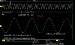
Fig 6 is a real waveform with 30kHz LPF of simple 12db/oct. You can see a little distortion. But they are above the audio band. I usually use 48kHz/24bit because my listening source is classic music recorded from 30's to 60's, they don't need high frequency. That's why my post-LPF is less important than 1bit DSM; simple RC is adequate.
Honestly speaking, I can understand the advantage of FIR DAC like Signalist but can't understand those of RNZ. I can make my new PCB with a discrete DSM DAC by the end of next month. Then, I will examine the advantage of NRZ. A real PCB is always a good guru who gives me much advice.🙂
My first choice is, as I wrote before, multi-bit DSM rather than 1bit.The analog post filter is also intended for multi-bit DSM(5 bit).I finally decided to use 7th order DSM implemented in FPGA. 7th of 1bit and 5bit have much difference in FFT like fig 1 to fig 4. Fig 1 is 1bit FFT without post-LPF, so-called NOS. Fig 2 is zoomed out to 3MHz bandwidth. You can see considerably high quantization noise as the theory says. This means the selection of post-LPF is necessary and essential. Fig5 is the reference of a real waveform with post-LPF. This is from SACD which has almost the same performance(a little bit less than fig 1). If you use a 30kHz cutoff, You can get less distortive one.
Fig 3 and 4 are 5bit DSM of 7th order(64OSR). Out of band noise is far less than 1bit. DSM usually uses high sample rate far beyond audio measurement instruments. If you want to check up to 3MHz(48kHz*64=3.072MHz), the best solution is a spectrum analyzer for RF. Attached are by MDO-3000. The noise floor is less performance for audio measurement. You can't measure SNR by this but spectrum to RF is reliable, not the best but better for DSM measurement.
Fig 6 is a real waveform with 30kHz LPF of simple 12db/oct. You can see a little distortion. But they are above the audio band. I usually use 48kHz/24bit because my listening source is classic music recorded from 30's to 60's, they don't need high frequency. That's why my post-LPF is less important than 1bit DSM; simple RC is adequate.
Attachments
Noob here, there is no upsampling so I guess this is can be considered a non-oversampling DAC ?
No, there is upsampling. Everything gets interpolated to 3 MHz sample rate by the SRC4392 and the FPGA module connected to J4 and J5.
Even 64 is adequate to eliminate quantization noise by simple 12dB/oct RC filter.
I just checked the out-of-band noise at the output of each filter stage in PWM8 mode:
First stage: about 15 mV quasi peak-peak single ended -> about 5 mV RMS differential
Second stage: about 10 mV quasi peak-peak single ended -> about 3.3 mV RMS differential
Third stage: about 20 mV quasi peak-peak single ended -> about 6.7 mV RMS differential (same as at the output of the complete circuit)
The second stage has a gain at low frequencies of 2.375 times and the low-frequency gain of the third stage is 1 time, so if you would amplify rather than filter the noise at the output of the first filter stage, the noise at the output of the whole thing would have been about 2.375 * 1 * 5 mV = 11.875 mV RMS rather than the 6.7 mV RMS there is now.
I think this confirms that I would not have lost that much by using a lower filter order, like you do.
I was a bit surprised that the out-of-band noise coming out of the third stage is stronger than the noise that goes in, but I guess this is due to the fact that the last stage has a relatively high Q factor.
- Home
- Source & Line
- Digital Line Level
- 74AHC02 and 74AHC08 DAC with 97 dB(A) dynamic range