Question from the newbie: would bypassing the output stage mean literally just running a few balanced mic cables from the main board to the XLR outputs?
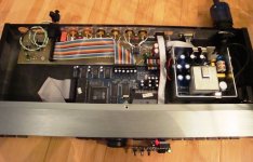
Still thinking of getting one of these, and it looks like just bypassing the output board yields a lot of improvement.
TIA
Chris
Yes, this is certainly possible, but you will probably want to add coupling caps to each line to prevent DC on the output.
If you have coupling caps at the input of any amps further downstream, then you probably could just buy some chassis mount XLR connectors and wire up a ribbon cable directly.
The above would indeed improve things (especially the extremely hot output levels), but the major problem is still the ASRC.
Regards,
Owen
Update
As an update for everyone else, I've basically shelved this project, and it's not likely to get revived.
Doing a new output stage and power supply will definitely help improve things, but no matter what you do on the output, the input ASRC is unacceptably bad, and the only way around this is implementing an external ASRC and tapping into the I2S lines on the DSP board. Clocks would also need to be replaced, and the modifications basically become impossible unless you really have a talent for SMD soldering and rework. It's certainly not a drop-in solution, and it needs to be if I'm going to make a board for people to use.
If the above were done, then you're basically replacing the entirety of the product with the exception of the DSP and user interface. It will be both costly and time consuming, and you still end up with a system that is less than ideal since the DSP only runs at 96kHz which means you always need an ASRC.
Running analog inputs is also not a solution, as the A/D converters are relatively poor, and if you're coming from an existing digital source, then this is forcing you into doing a D/A A/D D/A conversion which is also bad news.
Ideally, a proper DSP implementation should be able to run at whatever the native sample rate and bit depth of the material is, which would allow the system to work without up or downsampling. This, however, would require programming all filters for every possible sample rate, which is a bit of a task. It would also ideally use I2S for input and output, or at least use better DAC and ADC parts.
I think I will relegate the DCX to what it does best, which is prototyping and evaluating crossovers and system implementation. I will instead be implementing the necessary crossovers for my system using a simple active 4th order LR filter where I can decide on a crossover point with the help of the DCX, and then set the active crossover and remove the DCX from the system entirely.
Thanks to everyone for the interest, and feel free to keep discussions running on this page.
Cheers,
Owen
This is an excellent way to use the DCX..................... I will relegate the DCX ........................to prototyping and evaluating crossovers and system implementation. ...............where I can decide on a crossover point with the help of the DCX, and then set the active crossover and remove the DCX from the system entirely.....................
Many pictures, of course
I'd be very interested to the "one of them i build in a 6 channel preamp/volumecontrol based on 3 PGA2311 (very cheap 5.1 ebay Chinese)"
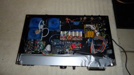
Here a pic of the 6 channel preamp DCX2496, without top..
and a passive out with digital in RCA replacement, out old board in this part, connect to DCX main board et voila, a very good sounding DCx2496
tojoko
Attachments
Any of you guys have a stock power supply that you pulled out of your unit that you would be willing to let go of? I am sure it is just laying around collecting dust anyway!
Thanks,
James
Hi Cloudbaseracer
I got a few and you can have one, where to?
tojoko
Great offer here but I need one in the United States. Anyone else have one they are not using?
Yes, this is certainly possible, but you will probably want to add coupling caps to each line to prevent DC on the output.
If you have coupling caps at the input of any amps further downstream, then you probably could just buy some chassis mount XLR connectors and wire up a ribbon cable directly.
The above would indeed improve things (especially the extremely hot output levels), but the major problem is still the ASRC.
Regards,
Owen
Hi Owen, thanks for that.
I'll probably be using the analogue inputs, so I don't think the ASRC will be an issue, but the ADCs might be. I'll see how it goes: my speakers need some line-level BSC and the sub needs integrating/eq'ing properly, so if I can get those sorted with less-serious problems elsewhere, I'll be happy.
Cheers
Chris
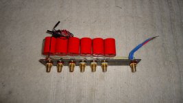
DCX2496 with 6 ch preamp remote controlled
A few more pics of closed box
Many pictures, of course
I'd be very interested to the "one of them i build in a 6 channel preamp/volumecontrol based on 3 PGA2311 (very cheap 5.1 ebay Chinese)"
A few more pics of closed box
Attachments
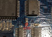
Something to think about
"If you do split the ground plane and run traces across the split, there will be no return path near the trace and the current will have to flow in a big loop. Current flowing in big loops produce radiation and high ground inductance." (More on that here)
"If you do split the ground plane and run traces across the split, there will be no return path near the trace and the current will have to flow in a big loop. Current flowing in big loops produce radiation and high ground inductance." (More on that here)
Attachments

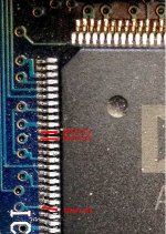
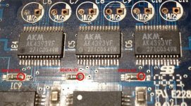
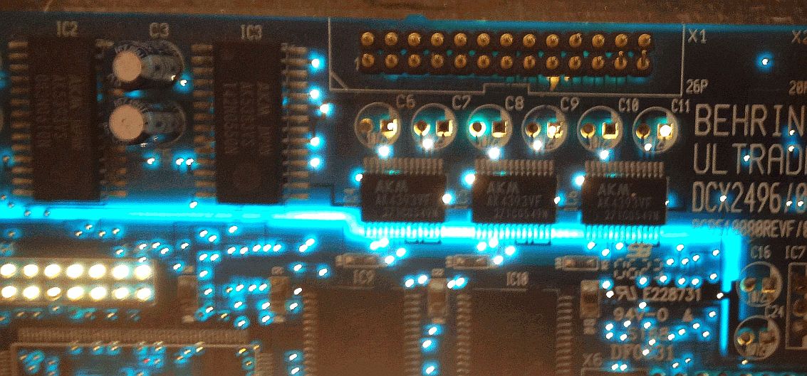
The split GND planes on the DCX board are there by design. Although I don't personally agree with this design decision, many DAC manufacturers still suggest it.
The purpose is to split the analog and digital return paths to avoid getting the high frequency digital return currents flowing through the analog plane.
If you look closely, you'll see that they don't actually run any critical traces across the gap between the planes, but that the DAC IC's do straddle the separation.
Again, this wouldn't be my personal approach, but it is very common practice and can provide some benefits if perfectly implemented under ideal conditions.
Cheers,
Owen
Obviously ...The split GND planes on the DCX board are there by design.

So it is. But in this case it is made in the absolutely worst manner.The purpose is to split the analog and digital return paths to avoid getting the high frequency digital return currents flowing through the analog plane.
What lines are critical if not clock and data lines?If you look closely, you'll see that they don't actually run any critical traces across the gap between the planes, ...
Where is their return path in that lousy design?It will provide essential benefits if implemented just right.Again, this wouldn't be my personal approach, but it is very common practice and can provide some benefits if perfectly implemented under ideal conditions.
Regards,
Gerd
Last edited:
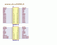
Does anyone have a link for the ribbon cable pinout to the output board? I'd like to make up some simple passive boards.
Also, has anyone changed the gain structure on the input board so that it matches the output at about +8dBU=0dBFS ? If I reduce my output gain by 14dB, I'm going to need about 14dB less attenuation at the input in order to have any reasonable signal level coming through.
Also, has anyone changed the gain structure on the input board so that it matches the output at about +8dBU=0dBFS ? If I reduce my output gain by 14dB, I'm going to need about 14dB less attenuation at the input in order to have any reasonable signal level coming through.
Try this. As far as converting the input, I followed Gary Pimm's design, and had good results. I have since gotten rid of it, and now go strictly digital in.
http://www.pimmlabs.com/web/behringer.htm
http://www.pimmlabs.com/web/behringer.htm
Attachments
Hello,
I've been searching around and not finding what I am looking for, and this thread seems as good as any. Thank you in advance!
I am looking for the simplest possible way to remove and eliminate the output board from the DCX and DEQ 2496's. The outputs will be easy, I will use the passive balanced out from this site:
Blanced passive output stage for the Behringer DCX2496
The question is, is there a passive circuit I can use for the INPUT side of both DCX and DEQ? Can I copy the same circuit and use for the inputs?
Analog must be used in my application, cannot be avoided.
Hi whiterabbit,
I'm not sure why you would need 8 transformers when the DCX and DEQ each only have 2 analog inputs.
Regardless though, I would avoid transformers as they are indeed expensive and don't bring anything to the table in this case.
For the input, the ADC needs each phase to be biased at half the analog supply voltage for the ADC. In this case, that's 2.5VDC.
The easiest way to accomplish this is to use a differential ADC driver like the OPA1632 and feed it's VCOM pin with a buffered 2.5V derived from the ADC analog supply through a precision resistor divider.
IIRC the input voltage on the ADC needs to be ~1.7VRMS for 0dBFS, so you need to adjust your gain according to whatever voltage you plan to feed the ADC.
If you really need to be passive, you might get away with a pair of decoupling caps, and two resistors after the caps connected to the derived 2.5VDC to bias the inputs to the ADC. I've never tried this, but it could work. It's likely you would still need a buffer for the VCOM voltage.
Regards,
Owen
- Status
- This old topic is closed. If you want to reopen this topic, contact a moderator using the "Report Post" button.
- Home
- Source & Line
- Digital Line Level
- DCX2496 Upgrade Board - Objectively Tackling the Improvement of a Stock DCX2496