A big issue is the thru plated holes. These just by themselves can be nonlinear resistances. Measuring real commercial boards filling the through plated holes with new solder did lower measured distortion. As a result it is wise not to use small vias that get completely filled during manufacture.
There's little need for a ground plane at all in an audio power amp - the frequency is too low.
That depends entirely on the precision level you're aiming to achieve. Here's one of Benchmark's engineers on the topic: Review and Measurements of Benchmark HPA4 Headphone Amp/Pre | Page 13 | Audio Science Review (ASR) Forum
Tom
If they‘re holes it will be funny passing reflow soldering and you would change immediatly to an other manufacturer. Sorry, but the last 20 years I‘ve no problem with holes in PCB!
JP
Even altium has a page on using high voltage on PCB layouts and how FR4 is inferior and the problems it can have:
High Voltage PCB Design Tips: Materials for High Voltage PCBs | Altium Designer
All good PCB manufacturers make more PCBs than you need, to ensure they can deliver working boards. No PCB process is perfect, that applies to materials and not just bad etching.
Why is that relevant here?
If someone places 100V differential traces or planes, easy on any class AB or D amplifier with +/-50V supplies, using 0.1mm or 0.2mm FR4 prepreg as an insulator, as you get on a chinese 4 layer stack up, you could have problems. If I was being really picky would stick with 2 layers to be safe, or segregate a design and have stuff below 50V with 4 layers + ground plane, and sections that are higher voltage without ground plane, and avoid using the inner 2 layers in that section.
Exactly, it is not even worth arguing about it. If someone thinks that ground plane is not needed, simply don't use it. I still be using ground plane most of the time for various reasons, some of which was mentioned here already.That depends entirely on the precision level you're aiming to achieve.
My two pennies - with careful consideration to layout you can use two layer boards for almost all audio work. I don't know if most people are careless when it comes to PCB design and therefore can't make two layers work to specification, or are just lazy and go straight for 4 layers to simplify things. I have been making my own two layer boards at home for many years and have rarely encountered a situation where a two layer board hasn't been possible.
This is from DACs to ADCs, USB interfaces, power amplifiers (class A, AB and D), DSPs, switch mode regulators, microphone preamps, LED drivers, motor drivers (sensorless sinusoidal three phase switching commutation, stepper motors etc) some of these being pretty high power and all without issue. Sometimes using a 0.4mm thickness board for impedance matching to the ground plane from top side traces where a 1.6mm board would simply require traces that are too thick for that to be possible.
I don't see why you cannot have a ground plane with a two layer PCB and creativity on the top layer. I regularly use 0 ohm 1206/0805 resistors to create the SMD equivalent of a link to keep almost all of my traces top side. This doesn't seem to hinder performance either as everything I make I measure and it better perform up to specification or I'm building it again. We're talking blameless power amplifiers with 0.0005% mid-band distortion, rising to 0.0015% towards the top of the audio band, TPA3251 class D chip amps performing to spec, AK4499 based DACs performing close enough to spec too (at least within my capabilities to measure it using a twin T notch, this is distortion below 0.0001%).
Would a 4 layer board make things a whole lot easier? Yes of course, in fact a three layer board would be the most useful, then I could add in a layer for power distribution alone. A 4 layer board would make things almost comically easy by comparison to the two layer, but I can't make those at home! In fact one of the biggest advantages to having a PCB fabrication facility make my boards would be with the vias. I use 1.00mm carbide micro drills for most of my drilling and go down to 0.8mm when necessary. I could probably go smaller now, I've built myself a semi-automated drill press just for drilling PCBs, but I haven't tried. The hand actuated drill press, using a regular drill, was just too crude for anything smaller otherwise the drills would break. This limits how small I can make a via from the top side down to the ground plane. Using a PCB fab that can drill 0.4mm (or smaller) with teeny tiny vias would allow me to build tighter layouts around small parts.
I have been designing my own PCBs for almost two decades though and have educated myself on the topic, both through reading literature and my own experience, towards the goal of getting as much performance out of my two layers as I can. If you're going to be using a PCB fab anyway, and don't mind the additional expense, just go for a 4 layer. You'll save time too. I can make a layout change and have a new board within a couple of hours. If I had to wait days, sometimes weeks, for a new revision to arrive from the fab plant I'd go mad.
From my perspective, and being able to build 2 layer boards at home, I would always try the two layer first and see what happens. If the part/project is going to be extra finicky about layout you'll usually learn a lot by building something with it. Just going for the 4 layer board isn't an automatic recipe for success, sometimes you need that experience too. I would start with 2 layers at home, learn from it, then go to an externally sourced 4 layer if its necessary to meet certain criteria. Usually the learning process has allowed two layers to suffice.
I don't know if most people are careless when it comes to PCB design and therefore can't make two layers work to specification, or are just lazy and go straight for 4 layers to simplify things. I have been making my own two layer boards at home for many years and have rarely encountered a situation where a two layer board hasn't been possible.
For me, it's performance and simplicity. But then, my layout strategy is rather more involved than simply connecting the dots.
I regularly use 0 ohm 1206/0805 resistors to create the SMD equivalent of a link to keep almost all of my traces top side.
Which works well for the hobbyist, but isn't a production solution. You don't have to use many 0 Ω resistors before the assembly cost associated with those resistors outweigh the added cost of going four layers.
TPA3251 class D chip amps performing to spec
Including emissions?
Would a 4 layer board make things a whole lot easier? Yes of course, in fact a three layer board would be the most useful, then I could add in a layer for power distribution alone.
Yeah... Many times I've wanted that third layer.
")
A 4 layer board would make things almost comically easy by comparison to the two layer, but I can't make those at home!
You can, actually. It's just much harder. I've heard of examples where a DIY 4-layer board was made by creating two two-layer boards and sandwiching them together. Painful, but it worked.
I have been designing my own PCBs for almost two decades though and have educated myself on the topic, both through reading literature and my own experience, towards the goal of getting as much performance out of my two layers as I can. If you're going to be using a PCB fab anyway, and don't mind the additional expense, just go for a 4 layer. You'll save time too. I can make a layout change and have a new board within a couple of hours. If I had to wait days, sometimes weeks, for a new revision to arrive from the fab plant I'd go mad.
I've been designing PCBs since I was in 5th grade, so for 30+ years now. I started with paper and DALO pen. I then moved on to a photolithographic process (I've used both positive and negative processes). Then toner transfer. And you're right. It's hard to beat the convenience of the garage fab, at least if you don't mind the mess. But, at the same time, it is also very easy to beat the capabilities of a garage fab.
Having through-plated holes is something I'd miss dearly with garage fab boards. And, as you point out, vias. Some features, such as the thermal vias under a QFN or LLP package are out of reach in a garage fab which imposes restrictions on your component choices.
With the prices and quality of low-quantity board runs from overseas and outfits like OSH Park, I just don't see any reason to maintain a garage fab. I haven't thrown the stuff out yet, but it'll probably go next time I move.
The wait is not too bad. I tend to have boards within a week or two. I spend the time on other tasks/projects.
I also tend to not have a lot of board iterations.But each to his own. We can all coexist.
Tom
Geez, these forum members are 'hotly' discussing the relevance of 4 layer PCBs to power amplifiers! This tentatively implies, an amplifier PCB would have the equivalent of 8 layers... Such unnecessary complications, make me doubt, whether technology has become some form of religion with no objectivity. If humans are NOT capable to PERCIEVE ultrasound, why does an amplifier need to have a bandwidth extending into MHz?! Provided the bandwidth is enough for high frequencies to be properly reproduced, there is no necessity.
For me, it's performance and simplicity. But then, my layout strategy is rather more involved than simply connecting the dots.
Yeah mine is too! You don't get the associated measured performance if all you're doing is connecting the dots.
Which works well for the hobbyist, but isn't a production solution. You don't have to use many 0 Ω resistors before the assembly cost associated with those resistors outweigh the added cost of going four layers.
Oh of course. If I were going production with any designs I'd go 4 layer all the way and go to a fab shop. I wouldn't home cook for anything I'd sell, except for the odd one off commission. That being said I got my idea for using zero ohm links from multilayer(!) commercial stuff. I was like 'oh yeah' of course you can do that - duh. In fact I didn't know zero ohm resistors even existed until I saw them being used on a PCI card. Then my world opened up
Including emissions?
I would assume so. TI only use two layers in their EVM for that chip and many other of their class D chips too. I seem to remember international rectifier also showing layout examples of single layer PCBs for some of their IRS20xx(x) chips - a how to use kind of thing. I think Hypex only use two layers in their UcD modules too. At least that's what it looks like with my UcD400 modules, their reliability not being what it should be... I've looked at the boards a fair bit
Yeah... Many times I've wanted that third layer.
You can, actually. It's just much harder. I've heard of examples where a DIY 4-layer board was made by creating two two-layer boards and sandwiching them together. Painful, but it worked.
I have considered doing that from time to time and indeed the prospect was not a pleasant one.
Having through-plated holes is something I'd miss dearly with garage fab boards. And, as you point out, vias. Some features, such as the thermal vias under a QFN or LLP package are out of reach in a garage fab which imposes restrictions on your component choices.
Get creative Tom! I've used many chips with thermal pads including high power LEDs on home brew boards. If the pad is big enough you can simply drill a hole in the PCB, 2-3mm in diameter. Solder the chip top side then flip the board over and solder the pad from behind with enough solder directly to the back of the board. The other option is using solid copper wire. For the high power LEDs I used a section of 1.5mm solid copper. File one end flat, chop off a length of 3mm or so, drill a 1.5mm hole in the PCB, push the copper wire into the hole, the flat filed end flush with the top side of the PCB. You get the idea, flat copper wire solders to pad, goes through PCB and solders to the back side. Using a suitable copper wire has better thermal conductivity than solder too.
I've also made home brew metal cored PCBs too, nothing elaborate mind you, you can buy the blanks from RS/farnell these days. Same process you just use a different etchant.
Cree have some application notes on using some of their high powered LEDs without MCPCBs. Exploring the thermal effects and performance of 1.6 and 0.8mm FR4 PCBs on their LEDs, some that do and some that don't have specific thermal pads. These are actually fairly high power 1 and 3 watt chips, some as small as 1.6mm square. The results are actually quite surprising and with a decent amount of top side copper area around the small LED pads you get a considerable amount of heat conduction through the PCB itself. So much so that you don't even need thermal vias if you have a decent sized top area connected to a thermally conductive pad.
You can find them here...
https://www.cree.com/led-components/media/documents/XLamp_PCB_Thermal.pdf
https://www.cree.com/led-components/media/documents/PCB_Thermal_XQ_XH.pdf
The wait is not too bad. I tend to have boards within a week or two. I spend the time on other tasks/projects.
I am impatient to say the least. Even if I used overseas fab for certain projects I'd home cook too for lots of things, at least to get things started, then move to overseas fab for the final push.
Sometimes I come up with an idea and want it done within a day or two. Or run into a tiny problem and need to make a small PCB to fix it. I'm not waiting weeks for that.
Geez, these forum members are 'hotly' discussing the relevance of 4 layer PCBs to power amplifiers! This tentatively implies, an amplifier PCB would have the equivalent of 8 layers... Such unnecessary complications, make me doubt, whether technology has become some form of religion with no objectivity. If humans are NOT capable to PERCIEVE ultrasound, why does an amplifier need to have a bandwidth extending into MHz?! Provided the bandwidth is enough for high frequencies to be properly reproduced, there is no necessity.
You can get basic blameless power amp performance from single sided PCBs.
Fully discrete power amps don't need, or even have a specific requirement for a ground plane. There simply aren't that many connections to a plane to be made or that much current that would flow into one. Most of the current flow is rail to rail and the speaker return needs to be directed 'star earthed' as it were to ensure performance.
Going double sided helps keep things more compact and allows you to keep heavy current traces short and direct. In fact, for audio, there's a lot to be said for going big. Usually the best way to ensure a reduction in cross coupling, from one part of a circuit to another, is space. Put distance between the two things if you can. Miniaturisation is great for some things but sometimes going bigger has its advantages.
Here is a recent experience I had, buying 4-layer PCBs from the Chinese fab named JLCPCB.
Tues, May 26, 3:40PM California time: Uploaded Gerber files to JLCPCB website
Wed, May 27, 07:40AM Shenzhen time: Received email acknowledgment from JLCPCB {see leftmost icon in Figure 1 below}
Sun, June 01, 10:14AM Shenzhen time: Fabrication complete. Finished PCBs boxed & placed on JLC's loading dock {see rightmost icon in Figure 1}
Sun, June 01, 5:33PM Shenzhen time: DHL picks up shipping box from fab {see BOTTOMmost line in Figure 2}
Tues, June 02, 12:31AM Hong Kong time: shipping box arrives at DHL sort facility in Hong Kong {see line item 6 of Figure 2}
Tues, June 02, 02:29AM California time: shipping box arrives at DHL sort facility in Los Angeles {see line item 11 of Figure 2}
Tues, June 02, 1:48PM California time: DHL rings my doorbell, obtains my signature, and hands me my box of thirty 4-layer PCBs. {see line item 19 of Figure 2}
-----------------------------
That's right. In 6 days + 23 hours, JLCPCB built thirty 4-layer PCBs, shipped them by DHL, and I received them at the front door of my home.
An hour less than 7 calendar days! You'll notice that these guys work hard even on the weekends. Amazing.
+
Attachments


Last edited:
Would be interesting to see the difference in an amp built using big through hole parts, and another with equivalent small SMD parts where possible (eg bc846 in place of bc546 transistors, 0402/0603 smd resistors where power allows). Compare the 2 side by side. The parts you could likely replace would be in the input stage, which should be the most influenced by the change.
SMD parts should be more susceptible to RF/EMC related interference, and might be better on a 4 layer ground plane design, possibly...
SMD parts should be more susceptible to RF/EMC related interference, and might be better on a 4 layer ground plane design, possibly...
Last edited:
That depends entirely on the precision level you're aiming to achieve.
An impressive EMI demonstration in a professional development course by Michael Schutten
of GE Research, showed very clear improvements with the use of a ground plane starting
above just 1kHz, with standard pcb material.
Last edited:
SMD parts should be more susceptible to RF/EMC related interference, and might be better on a 4 layer ground plane design, possibly...
Should they? I'd say they are smaller, so they are worse aerials/antennas, so you get less interference problems.
If humans are NOT capable to PERCIEVE ultrasound, why does an amplifier need to have a bandwidth extending into MHz?! Provided the bandwidth is enough for high frequencies to be properly reproduced, there is no necessity.
For the same reason why audio op-amps always have gain-bandwidth products in the megahertz range. For example, suppose you want to make a feedback amplifier that has a simple single dominant pole compensation and (in order to keep the distortion for high audio frequencies low) a loop gain of 100 at 20 kHz. Do the math and you will find that the bandwidth is (at least) 2 MHz. Of course you can restrict the bandwidth with passive filters at the inputs and outputs, and doing so will reduce the chance of receiving broadcasts you didn't want to receive, but the basic amplifier has a 2 MHz bandwidth.
I'd say they are smaller, so they are worse aerials/antennas, so you get less interference problems.
Definitely. Ground planes are more effective with smt packages, also.
It's not just the components, it's how they interact with the PCB traces and layout in general. Small SMD parts have some funky behaviour at high frequencies (like 4G and WiFi frequencies which are abundant these days) - resistors can become inductive and capacitors have low impedance, it can have unexpected interactions with a circuit when the parts don't work as expected. Assume with something like an audio amp that will result in more output noise - you can get that by placing your mobile next to some equipment.
... audio op-amps always have gain-bandwidth products in the megahertz range.
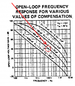
The integrated circuit opamp called uA741 (released 1969) has a gain bandwidth product of 1.0 MHz. It is internally compensated to be stable at a gain of 0dB (1X). The integrated circuit opamp called uA709 (released 1965) has a gain bandwidth product of 10.0 MHz at a gain of 40dB. It is externally compensated. See red circle below.
_
Attachments
It's possible to do decent audio designs on single layer boards. A lot of commercial designs use single layer boards because of the cost factor (gotta oinch those pennies...). I generally use 2-layer designs as it makes life a little easier, and it's the default option for my PCB vendor. The only time I might consider a four layer design would be if I wanted to try my hand at designing a DAC.
SMPS designs are quite often done on single-sided boards because of cost. It's possible to do a good design that way, with a sprinkling of jumpers where needed.
The commercial sector also pinches pennies by using cheaper substrate material than FR-4, like phenolic or CEM-1 (paper-epoxy). The phenolic boards are the cause of that classic "new electronics" smell when you pop open the box on a new piece of gear..
- Home
- Design & Build
- Construction Tips
- Two layer versus four layer PCBs