Hi all,
with JLE TPA3255 amp in the table, i am trying to shunt the input stage, which is unuseful because drived with a high level differential DAC (SMSL SU-9).
The JLE amp is design with PFFB topology.
Tried yesterday shunting input stages not working. Amp goes to FAULT.
What i had done :
Something strange is near 2.9V DC mesured at the outputs AC blocking caps.
Another try is removing 100k input resistors to ground (RA1, RA2, RB1, RB2). Same results.
with JLE TPA3255 amp in the table, i am trying to shunt the input stage, which is unuseful because drived with a high level differential DAC (SMSL SU-9).
The JLE amp is design with PFFB topology.
Tried yesterday shunting input stages not working. Amp goes to FAULT.
What i had done :
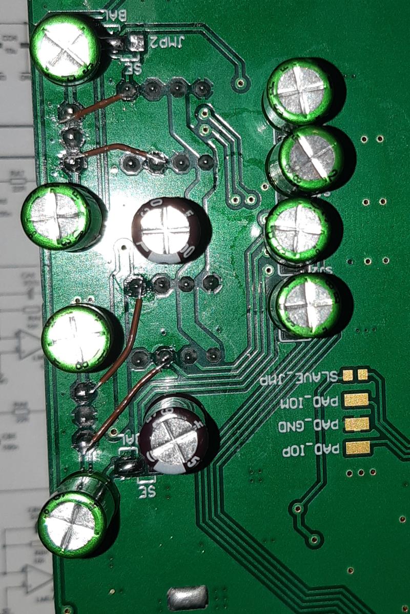
- Remove SE/BAL solder jumpers
- Remove opamps from sockets
- Connect J1-1 to socket A pin 1
- Connect J1-3 to socket A pin 7
- Connect J2-1 to socket B pin 1
- Connect J2-3 to socket B pin 7
Something strange is near 2.9V DC mesured at the outputs AC blocking caps.
Another try is removing 100k input resistors to ground (RA1, RA2, RB1, RB2). Same results.
D
Deleted member 148505
D
Deleted member 148505
Something strange is near 2.9V DC mesured at the outputs AC blocking caps.
Each IN_X of TPA3255 pin sits at the Vmid of AVDD (internal opamp supply) so this is normal. There is 100 ohm series to each cap so you are measuring lower voltage.
Ahh, i did not see that. Then the issue should be too much common mode between the pinuts and mid internal supply of the TPA ?
Should i put 1k between in+ and Agnd (mid_V) and another between in- and Agnd (mid_V) ?
In this cas, if it works, shall i put some DC coupling caps between the dac and the board (may be not) ?
Should i put 1k between in+ and Agnd (mid_V) and another between in- and Agnd (mid_V) ?
In this cas, if it works, shall i put some DC coupling caps between the dac and the board (may be not) ?
D
Deleted member 148505
Ahh, i did not see that. Then the issue should be too much common mode between the pinuts and mid internal supply of the TPA ?
Should i put 1k between in+ and Agnd (mid_V) and another between in- and Agnd (mid_V) ?
In this cas, if it works, shall i put some DC coupling caps between the dac and the board (may be not) ?
1K is too low. Then if you put DC coupling caps, removing buffer opamps will be pointless because I think DC coupling caps has more effect on the sound than the opamps, and the opamps help by filtering out high frequency input.
With the same modifications as yours (first post), I tried my external balanced driver (isolated DC-DC dual supply + THAT 1646) and it works, the amp starts without problem.
Regards,
Lester
D
Deleted member 148505
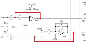
Here is bypassing of opamps if you want it with blocking caps.
You can safely connect your DAC with this config.
The amp will not start though if there is no source connected.
You can safely connect your DAC with this config.
The amp will not start though if there is no source connected.
Attachments
Last edited by a moderator:
Agree for the pointless with 2 DC coupling caps.
I thought about line driver and i should received a homemade pcb with DRV135, in case of SE configuration. My PCB should be supply by external split supply; delivered by the main SMPS supply (one 48V and one small +/12V), and regulated by TPS7A49 et TPS7A30.
I plan to test it next week. Big work to suppress just one cap ...
It let you know that ThatCorp recommand the split supply (for 1646) instead of TI does not recommand it with DRV135 ...
D
Deleted member 148505
Agree for the pointless with 2 DC coupling caps.
I thought about line driver and i should received a homemade pcb with DRV135, in case of SE configuration. My PCB should be supply by external split supply; delivered by the main SMPS supply (one 48V and one small +/12V), and regulated by TPS7A49 et TPS7A30.
I plan to test it next week. Big work to suppress just one cap ...
Yes if you have an external aux split supply it will be easier to bypass the onboard buffers and caps.
I expect it to perform better than the onboard buffer because of low noise regulators that you will use.
D
Deleted member 148505
I already received 10uF, 50V Panasonic FR. I soldered it on TPA3255 input side. My initial impression is that it has the same smoothness as Elna Silmic II, treble is good. I haven't figured out its sound signature yet.. I need more sound comparison 🙂
Are you talkin about decoupling caps ? If yes, i studied them a bit, 20 years ago 🙂eek🙂, and my reference was Oscon caps in terms of ESR.
Then your best suggestion is to dual supply the buffers.Yes if you have an external aux split supply it will be easier to bypass the onboard buffers and caps.
I expect it to perform better than the onboard buffer because of low noise regulators that you will use.
2 solutions for me. Aux supply already present in my SMPS or build an inverter with 12v embedded in the TPA amp board. In this last case,i think to LT3462.
In both case, very good regulators should be TPS7A47 and TPS7A33.
This implies a custom PCB, then the possibility to change to OpAmp topology.
SE or Balance are possible. I can use both.
Balance avoids an opamp pass in my configuration (SMSL SU-9) and i think it is more accurate to use 2 inverter buffers instead of 1646/DRV134, following to their datasheets. At least, inverter buffer ... Or non inverting shall have a bit less noise, following to TI TINA simulation.
If inverter option to be use, INA1620 should be great (better CMRR due to embedded resistors and PSRR due to GND pin).
Your opinion ?
D
Deleted member 148505
looking for advice for kits you selling on Ebay?
I'm sensing a mockery here 😱
D
Deleted member 148505
You can also try OPA1632 or OPA1637.
Then your best suggestion is to dual supply the buffers.
2 solutions for me. Aux supply already present in my SMPS or build an inverter with 12v embedded in the TPA amp board. In this last case,i think to LT3462.
In both case, very good regulators should be TPS7A47 and TPS7A33.
This implies a custom PCB, then the possibility to change to OpAmp topology.
SE or Balance are possible. I can use both.
Balance avoids an opamp pass in my configuration (SMSL SU-9) and i think it is more accurate to use 2 inverter buffers instead of 1646/DRV134, following to their datasheets. At least, inverter buffer ... Or non inverting shall have a bit less noise, following to TI TINA simulation.
If inverter option to be use, INA1620 should be great (better CMRR due to embedded resistors and PSRR due to GND pin).
Your opinion ?
I already received 10uF, 50V Panasonic FR.
FR have a hard sound...no warm....no good
D
Deleted member 148505
Test ongoing ...
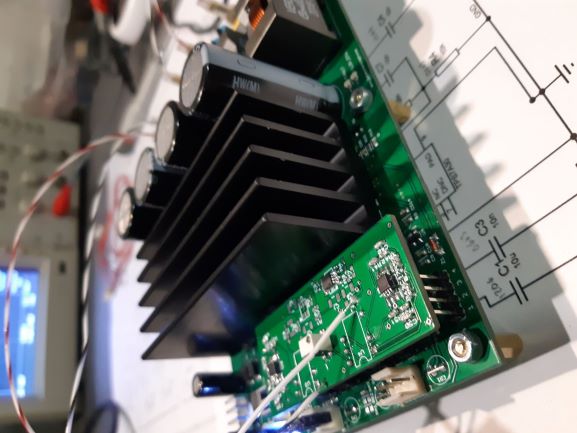
https://goopics.net/i/YlXN2
Looks good! What's the power consumption of your board?
FR have a hard sound...no warm....no good
Yup silmic II is still better
I did not measure et and i have to replace an OPA1637 which i have destroy. VSSOP is a real nightmare to solder. I will give the board to a professionnal guy at work on monday for that.Looks good! What's the power consumption of your board?
Theorically:
2xOPA1637 : 2x0.95mA quiescent current. Zin of TPA is 26K then current should be quite low.
TPS7A30 (to regulate -12V to near 11.5V) : near 55 to 100uA
TL3462 (to invert +12v to -12V) : 2.9mA plus output_current*efficiency(75%) then may be 6mA max
To conclude may be 6mA.
I will do not forget to measure if you want.
- Home
- Amplifiers
- Class D
- JLE TPA3255 Build and Modifications