Sorry, I missed this. I do not know enough about PCB manufacturing to say if the PCB is ENIG or not.wondering PCB not ENIG?!
JP
I mapped out the MCU pin connections on the topping. It is very confusing. They used an MCU with dedicated I2C pins. But the I2C pins are set to be generic GPIO and one of them appears totally unused.
Actual I2C connections are made to PWM/Onboard crystal oscillator pins.
There is UART breakout for some unknown reason. Potentially more GPIO, but the header to which they are connected is:
[ TX | RX | RST | SWIM | GND | VDD ]
The I2C connections are broken out on another 4-Pin header but the pinout is:
[ SCL | SDA | FLOAT | FLOAT ]
The datasheet mentions that the MA12070's /CLIP pin can be high state to signal the MCU to increase drive voltage or attenuate digital volume, but topping looped the /CLIP pin to ground through an RC. However, two pins (outside of the voltage block of the MCU) connect to the IVR/Linear reg section of the board???
Red = Topping Connection. Green = ST Micro pin usage.
- The I2C pin 12 (SCL) can be: GIPIO, I2C, or ADC external trigger.
- I2C Pin 11 can be: GPIO, I2C, Timer 1 break input.
- It almost looks like they had an idea because SCL is on ocsillator input. Both chips are configured with an identical I2C address. Not sure how this would work with the ACK from slave devices. Both chips have an identical I2C config which is odd.
They seem to be bit banging via GPIO (IF any I2C communication is actually happening). But why Topping would do that on literally the lowest power STM8s device available is beyond me. There are perfectly good I2C pins as part of the MCU! I guess it's time to try coding. I don't really want to try rearranging traces.
First shoot.
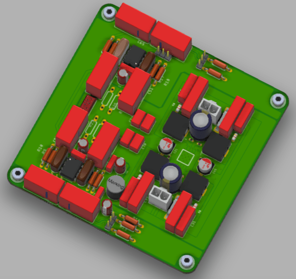
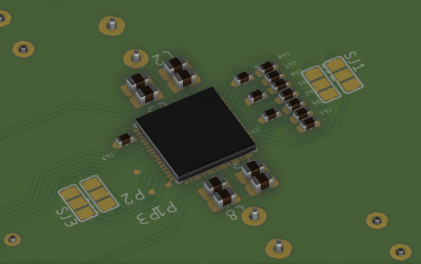
Seems to fit 100x100mm 4 layer PCB (signal, power, power, signal).
Mixed THT and SMD (not so much) components: MA12070 on bottom layer, small area on top side for small BGA heatsink (IMO, inner layers copper sufficient).
10µF as film THT (MKP4) or Al.-Elyt. THT (ELNA RFS end of life unfortunately).
All recommended filters on board as variants.
No I2C interface routed.
Power supplies (PVDD, VDD, AVDD, +12V) and SE/DIF connectors (thinking about MicroMatch for XLR/RCA rear panel PCB) missing.
MicroMatch for front panel PCB with ERROR (LED), CLIP (LED), ENABLE (switch) and RESET (switch).
WE MPC4 to binding posts.
FE from TPA32555 (dual OPAMP).
JP
Seems to fit 100x100mm 4 layer PCB (signal, power, power, signal).
Mixed THT and SMD (not so much) components: MA12070 on bottom layer, small area on top side for small BGA heatsink (IMO, inner layers copper sufficient).
10µF as film THT (MKP4) or Al.-Elyt. THT (ELNA RFS end of life unfortunately).
All recommended filters on board as variants.
No I2C interface routed.
Power supplies (PVDD, VDD, AVDD, +12V) and SE/DIF connectors (thinking about MicroMatch for XLR/RCA rear panel PCB) missing.
MicroMatch for front panel PCB with ERROR (LED), CLIP (LED), ENABLE (switch) and RESET (switch).
WE MPC4 to binding posts.
FE from TPA32555 (dual OPAMP).
JP
Progress today.
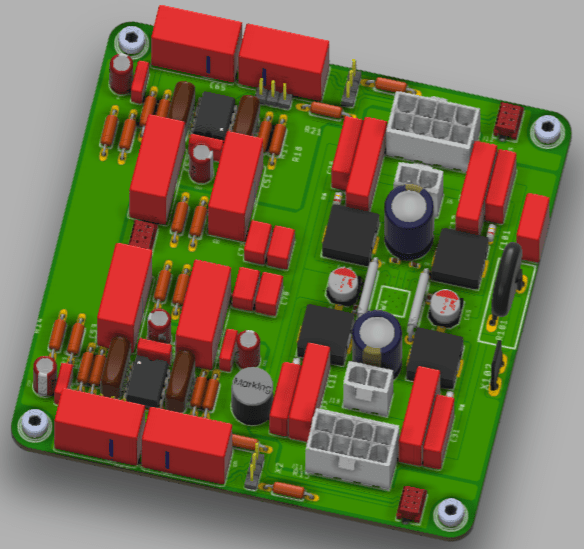
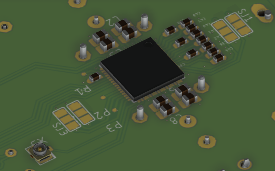
Ground lift.
WE MPC4 for power input and power through (daisy chaining).
The board allows SE or DIF input to BTL and DIF input to PBTL (two metal jumper from fischer elektronik added but wires are fine too).
u.fl connector added for multiple boards synchronization (Master/Slave).
JP
Ground lift.
WE MPC4 for power input and power through (daisy chaining).
The board allows SE or DIF input to BTL and DIF input to PBTL (two metal jumper from fischer elektronik added but wires are fine too).
u.fl connector added for multiple boards synchronization (Master/Slave).
JP
Must be overlooking it in the design guide V1.2 from 26-5-2021 as I only see the recommended common mode filtering and the caps. I don't see why upping the PSU impedance will do good.
It says to use a common mode choke in the range 2x40 μH to 2x100 μH + a capacitor in the range of 100 nF to 220 nF. Or CLC with
ferrite BLE32PN300SN1L and 2 x 22 nF.
It says to use a common mode choke in the range 2x40 μH to 2x100 μH + a capacitor in the range of 100 nF to 220 nF. Or CLC with
ferrite BLE32PN300SN1L and 2 x 22 nF.
Looks pretty good to me.
Any reason you seem to separate PVDD and AVDD into different supplies? A single well-filtered supply and a decent linear reg onboard would seem to be easier and less expensive than a discrete very clean AVDD supply (though unsure if layout permits)? Or perhaps you also have a PSU design to couple with it which would be really neat!
A couple Topping PA3s updates:
- Topping read-protected the MCU. No easy way to dump the code without HW hacking.
- I asked topping if they would be willing to share an always-on firmware. My hopes are not high even though it would probably be <5 lines of code to change.
- I really want to connect the epads and swap the heatsink to the other side. Infineon shows serious gains to be had by keeping junction temperature lower.
Linear regulators suffering availability. So I prefer separating amplifier (except MA12070, mainly discrete components) from PSU.
For the PSU, I´m thinking about LT/AD silent switcher and LT/AD low noise regulators, but I´m always braining.
Perhaps that someone has an idea for the way to go?
JP
For the PSU, I´m thinking about LT/AD silent switcher and LT/AD low noise regulators, but I´m always braining.
Perhaps that someone has an idea for the way to go?
JP
Oof, I see that now. Some of the switching regs have a cleaner output. Thinking Omsemi and TI which have outputs with uV ripple and uA quiescent. If those are properly implemented they might work. Not sure on the AD/DC conversion since it would be country specific but the switching regs might work well, and they would have greater efficiency.
Also looked at the design (but not enough). Some things:
- input capacitors could be film types just as the flying capacitors.
- Flying caps can be 4.7 µf film types as ceramic 10 µF types are chosen and datasheet says half the value counts with DC bias.
Effective capacitance should be minimum 4.0 μF at 0.5*PVDD voltage. Wima 4.7 µF 50V will do OK. Is their ESL too high?! - if the flying caps stay X7R please make them 50V or better 100V types or you'll hear them making music.
- since an external PSU is considered a 2 x 7V or 2 x 9V 5 to 10 VA toroid is a possibility. Then the opamps could be fed +/- 7...9V and coupling caps could then be omitted. It would also make 2 x 5V possible with low loss in heat and no HF/RF from either switchers or noisy PVDD. It would require some coils and own regulators though to separate the opamps PSU.
- onboard volume control or at least the pads for RK27 or even 4 gang RK09 footprint would be a blessing.
- please consider the 1 µF caps to be all 2.5 mm pitch film types.
- the input filter at MA12070 is a novelty (curious what they will bring) but please also consider an input RC filter.
- Linear regulators (even older noisy ones) for the 5V are an immediate improvement over the standard noisy switchers on ready made boards so that is the way to go I think. No experiments done with 2 x 5V. Problem with linear regulators is the about 1W loss in heat due to 26V PVDD.
- My MA12070 devices that are sacrificed for science all react well to a 19V 5A linear PSU. An improvement over the included SMPS. My design idea was a local linear regulator. My current test device has a 17V 5.6A industrial (hence the unusual values) toroid, Schottky diodes, 15,000 µF and a linear regulator set at 20V.
- OPA1642 really is a good opamp for the purpose.
Last edited:
erratum: My current test device has a 17V 5.6A industrial (hence the unusual values) toroid, LT4320 ideal rectifier, 15,000 µF and a linear regulator set at 20V.
Please note that even 7805 is an improvement over the more or less standard switcher circuits as done on cheap boards. A combination of switcher from PVDD 19...26V set at let's say 9V output, a CLC and then an ultra low noise SMD LDO 5V regulator is an option (but it will cost more). Or the same done with a 7805 if it needs to be cheap.
Local regulator (5V) close to the MA12070 is advisable. Think of the MA12070 as a nice sounding EMI transmitter.
Last edited:
Could you told me where do you want to place the volume control regarding to my schematics?Also looked at the design (but not enough). Some things:
- input capacitors could be film types just as the flying capacitors.
- Flying caps can be 4.7 µf film types as ceramic 10 µF types are chosen and datasheet says half the value counts with DC bias.
Effective capacitance should be minimum 4.0 μF at 0.5*PVDD voltage. Wima 4.7 µF 50V will do OK. Is their ESL too high?!- if the flying caps stay X7R please make them 50V or better 100V types or you'll hear them making music.
- since an external PSU is considered a 2 x 7V or 2 x 9V 5 to 10 VA toroid is a possibility. Then the opamps could be fed +/- 7...9V and coupling caps could then be omitted. It would also make 2 x 5V possible with low loss in heat and no HF/RF from either switchers or noisy PVDD. It would require some coils and own regulators though to separate the opamps PSU.
- onboard volume control or at least the pads for RK27 or even 4 gang RK09 footprint would be a blessing.
- please consider the 1 µF caps to be all 2.5 mm pitch film types.
- the input filter at MA12070 is a novelty (curious what they will bring) but please also consider an input RC filter.
- Linear regulators (even older noisy ones) for the 5V are an immediate improvement over the standard noisy switchers on ready made boards so that is the way to go I think. No experiments done with 2 x 5V. Problem with linear regulators is the about 1W loss in heat due to 26V PVDD.
- My MA12070 devices that are sacrificed for science all react well to a 19V 5A linear PSU. An improvement over the included SMPS. My design idea was a local linear regulator. My current test device has a 17V 5.6A industrial (hence the unusual values) toroid, Schottky diodes, 15,000 µF and a linear regulator set at 20V.
- OPA1642 really is a good opamp for the purpose.
JP
I bow to Jean-paul's knowledge, but a couple thoughts of my own. The design looks fairly straight forward data-sheety just with some nicer bits.
Regarding the flying caps:
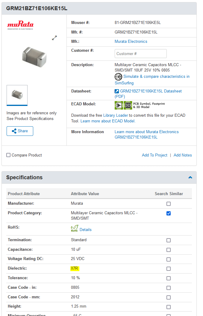
"Care must be taken when choosing flying capacitors in applications where maximum output power is needed. The
effective capacitance of poor ceramic capacitors can be greatly reduced when a DC bias voltage is applied. A
recommended part is the GRM21BZ71E106KE15L capacitor from Murata. Other parts may also be used as long as the
effective capacitance is minimum 4.0 μF at 0.5*PVDD voltage."
I agree that a cheap cheap switching power arrangement may perform poorly, but some switchers range are recommended for use in instrumentation designs (measuring equipment) where they are used as voltage comparators. I think these applications are a touch more demanding than a chipamp.
Many linear regs have output voltage error in the 100mv region whereas something like the lt8683s has a 10mV ripple w/o further filtering and operates in the MHz (inaudible) range. AVDD doesn't have many transients so the wildly low ripple voltage (<10Vpp) seems like a great match.
All that said, a decently implemented switching power supply can be less noisy than a linear reg (by a lot) but the cost will be much higher and implementation more difficult. There's a lot of math (start at page 12 of this https://www.analog.com/media/en/technical-documentation/data-sheets/lt8609s.pdf) and implementation will be entirely application dependent (one PSu will not go between projects).
Here's some more data with measurements: https://www.audiosciencereview.com/...r-supply-with-a-smps-incl-measurements.36536/
Regarding the flying caps:
"Care must be taken when choosing flying capacitors in applications where maximum output power is needed. The
effective capacitance of poor ceramic capacitors can be greatly reduced when a DC bias voltage is applied. A
recommended part is the GRM21BZ71E106KE15L capacitor from Murata. Other parts may also be used as long as the
effective capacitance is minimum 4.0 μF at 0.5*PVDD voltage."
I agree that a cheap cheap switching power arrangement may perform poorly, but some switchers range are recommended for use in instrumentation designs (measuring equipment) where they are used as voltage comparators. I think these applications are a touch more demanding than a chipamp.
Many linear regs have output voltage error in the 100mv region whereas something like the lt8683s has a 10mV ripple w/o further filtering and operates in the MHz (inaudible) range. AVDD doesn't have many transients so the wildly low ripple voltage (<10Vpp) seems like a great match.
All that said, a decently implemented switching power supply can be less noisy than a linear reg (by a lot) but the cost will be much higher and implementation more difficult. There's a lot of math (start at page 12 of this https://www.analog.com/media/en/technical-documentation/data-sheets/lt8609s.pdf) and implementation will be entirely application dependent (one PSu will not go between projects).
Here's some more data with measurements: https://www.audiosciencereview.com/...r-supply-with-a-smps-incl-measurements.36536/
Eh ... I meant the usual switchers on various MA12070 boards to convert 26V to 5V. Those are easily outperformed by even 7805 with its average 50 ...100 µV of noise. I would choose an SMD low noise LDO though. Smaller, closer to the chip, lower noise...Issue is the 26V to 5V that will create useless heat when using linear regulators. Does not correlate with the energy efficient MA12070.
2 Channel volume control can be in front of the first opamp as I guess (assumption alarm!) that most have unbalanced setups. When wanting balanced inputs probably a preamp/DAC with balanced outputs and internal volume control will be used?! If true these won't bite each other.
MKS for flying caps is a bit of a gamble hence my question about ESL. I haven't dared to implement them on my boards (yet) as the lead wires definitely will be too long (rework of existing PCB) but decoupling with MKS is quite good. All is concentrated on low cost in the datasheet as the chip is intended for low cost devices. Somewhere some words are spent on using film caps. The stated minimum voltage rating is 25V. I have one amplifier where they make noise.
Datasheet just says:
"The two flying capacitor terminals are to be considered high power switching nodes carrying voltages and currents similar to that on the OUTXX nodes. Care must be taken in the PCB design to reduce both the inductance and the resistance of these nodes."
Again, the total cost of an amplifier board as stated by Infineon is 2.15 $ based on 1000 pieces. That is PCB, all parts and assembly and less than a plastic meal at mcDonalds. You won't read anywhere to use better or overdimensioned parts
Last edited:
- SE/DIF OPAMP with +6dB amplification following
- by 100k stereo volume potentiometer
- following by +9.5dB DIF OPAMP amplification
- allows +15.5dB amplification
- supplied by +/-15VDC
1. is a choice but I think I need a schematic to correctly understand. I would leave away superfluous stuff. One opamp less -> less = more.
2. Why 100 kOhm? 10 or 20 kOhm means less noise and all sources of the last decades can drive that.
3. is a choice and easily changed.
4. IME the MA12070 has more than enough gain. NB: I noticed my theory around balanced + symmetric to be too rusty so no comment really.
5. Why? I know it is standard but with 2V rms sources it is not that necessary. It is OK though but it makes the 2 x 5V a new challenge. If you want all to be excellent you will end up with a 5 VA 2 x 7V, a 5 VA 2 x 12..15V and a 50...100VA 18V transformer
Suggestion: since the costs for power supplies for this IC quickly go wild maybe it is a good idea to first focus on this section. In my test setup the transformer and regulator already cost too much when compared to the ready made good devices. The challenge is clean 19....26V 5...8A, clean 5V (x2?) 200 mA and clean +/- 7....15V 100 mA.
Tomorrow I'll receive a Sabaj A10a with MA12070. Curious what 135 Euro will bring.
Last edited:
- Home
- Amplifiers
- Class D
- Infineon MA12070 Class D