I am also interested in this chip, has there been any progress getting a register map for the DSP registers? I would like to make a single board 8 channel amplifier with DSP using this IC but would need to be able to configure it from another microprocessor. The idea is a kind of single board sound system, just add speakers (and at low cost). I would be using one IC per channel in PBTL.
They have recently published that document, that describes (at least some) DSP registers. I did not had a deep look at it yet:
http://www.ti.com/lit/an/slaa799a/slaa799a.pdf
JMF
http://www.ti.com/lit/an/slaa799a/slaa799a.pdf
JMF
They have recently published that document, that describes (at least some) DSP registers. I did not had a deep look at it yet:
http://www.ti.com/lit/an/slaa799a/slaa799a.pdf
JMF
awesome this looks great and seems to have all the registers. It also answered a few things I was unclear on:
1. 15 biquads per side in 2.0 mode so no point running PBTL unless needing 2ohm capability.
2. Has a mono mixer so all chips can be supplied with raw stereo audio data
without needing any other DSP.
3. 48Khz is clearly optimal internal rate and it has a SRC.
It will be some time before I can start this project, someone will probably do it before me considering the popularity of mini DSP etc.
So, after discussion here TPA3255 - all about DIY, Discussion, Design etc., I decided to go to 10 mH and 0.68 uF for the output LC filter.
I have practiced since last year with solder paste and hot air reflow station. Now I feel OK soldering the ground pad of the LM5010. My limited skills in design make me infortable taking the risk to use a different implementation of something proven. So I will revert to the EVM configuration LM5010 and LM2940. Last a TLV1117-33 for the 3.3V.
I have now to modifiy my schematics and PCB.
JMF
I started looking at this again and notice that this chip does not have a large delay pool. Only 16 samples maximum delay (0.33 mS) so a small FPGA will be required for my intended use to implement a delay pool and coordinate the system. I would consider an MCU but I intend to drive at least 4*tas3251 so IO demands will swamp it. MAX10 looks like a decent choice. A larger FPGA would allow FIR filtering etc. but greatly increase cost and time to implement.
If it is only about delaying of x samples, this does not reauires a lot of CPU power. Stm32 MCU, able to manage several I2S should be suitable in my understanding.
By the way, I have finalized the PCB (trying to have some cross checks). Moment of truth approaching...
JMF
By the way, I have finalized the PCB (trying to have some cross checks). Moment of truth approaching...
JMF
Ok MCU's have got a lot more powerful in the past few years!
https://www.st.com/resource/en/datasheet/stm32h742zg.pdf
This looks like it could be a better choice than an FPGA. Even has an SPDIF receiver so can reduce chip count. 480MHz with 'DSP' instructions (I'm assuming multiply accumulate) should also result in a few biquads.
Excited to see your progress.
I have an implementation of a stm32F7 that implements Async USB input, DSP for LX-Mini speakers filtering, and controlling 2x Spdif out. This works quite well.
JMF
JMF
I have an implementation of a stm32F7 that implements Async USB input, DSP for LX-Mini speakers filtering, and controlling 2x Spdif out. This works quite well.
JMF
I have encountered a bit of an issue; I want to drive 4*TAS3251 and have SPDIF/AES inputs and analog inputs (stereo) so I need 6*I2S but the STM32F7 has only 4 I2S. Any ideas?
Hi,
I won't be able to help much more that what I write below, but the stm32f746zg has 7xI2S:
- 3 I2S (maybe possibility to configure one as SPDIF input ?),
- 2 SAI able to manage each 2xI2S (or SPDIF).
This is super cool for digital audio applications.
STM32F746ZG - High-performance and DSP with FPU ARM Cortex-M7 MCU with 1 Mbyte Flash, 216 MHz CPU, Art Accelerator, L1 cache, SDRAM, TFT - STMicroelectronics
The Nucleo development boards expose all pins and are cheap:
NUCLEO-F746ZG - STM32 Nucleo-144 development board with STM32F746ZG MCU, supports Arduino, ST Zio and morpho connectivity - STMicroelectronics
You can find information about the quite versatile SAI module here https://www.st.com/content/ccc/reso...nt/translations/en.STM32F7_Peripheral_SAI.pdf
The thing you have to pay attention is the different clock masters for inputs and outputs. This is key and there are different ways to address this. The one (and only one) I implemented is asynch USB.
Last, there is an agreement between ST and Audioweaver, so you can use that product on stm32 platform (I did not explored license limitations).
So not so bad 🙂
JMF
Hi all,
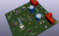
A small update here. After a loonnng summer, and lot of professional workload, a forced break helped move forward with this project.
I had some support from Doctormord and Voltwide to identify design flaws and possible improvements. I did my best to implement their advices. I double checked the things, and I'm ready to go to manufacturing. Time to jump now 🙂
The design intends to be compact, still cost effective for a DAC/DSP/Amp integrated option, with audio grade components (Wurth coils, premium/good caps, TI EVM level design).
JMF
Attachments
What is your plan for loading in DSP code? An external microcontroller?
Also, which heatsink are you planning on using?
Also, which heatsink are you planning on using?
Hi,
I see 2 scenarios:
1) connected direcly to to a Raspberry Pi, that would control the DSP, GPIO and provide the I2S flux,
2) connected to an external micro-controller. This is the easiest for me, as it is very similar to my current set-up with a STM32 Nucleo dev board.
Another option would be to include a small micro-controller on the board to manage the DSP controls and the GPIO, but then there is the question of hpw to control volume...
My need is for active speakers; with at least 2 amps. So having one central brain (uC or RPi) makes sense.
I think that I personally will go with 2)
JMF
GVDD_A testpoint breaks up the GND-fill alot, i'd put all testpins on the bottom side to have shortest connections. I'd recommend a testpoint with integrated VIA drill to have some sort of "locking" to the probe.
The DSP code needs almost no processing power, the most simple 8 bit micro can do the job. A board with wireless connectivity and an I2S bus would really add value. Something like a Raspberry Pi Zero W might be a good candidate. Maybe even a ESP32 would suffice. If you only need the bare basics to load the DSP code and control volume registers something like a Arduino NANO is okay. All options require quite some code for a full working solution.
@Doctormord: thanks => will follow your advice
@tschrama and Lutkeveld:
The functions to achieve by the "controller" are (at least):
- manage power ON sequence,
- manage the Power OFF sequence,
- manage FULT and RESET_AMP
- load DSP coefficients and other parameters,
- manage volume,
- possibly provide the USB to I2S translation, or BT to I2S, or...
Many options to do all of the above, some of them requiring very low CPU power.
The question is whether there is a huge benefit to have something onboard, or to be more on a daughter board approach.
The initial idea was to develop a "versatile brick" possible to use in many configurations, as opposed to the "plug and play digital amp". This better fits with the daughter board way...
But I'm interested in listening to others opinions.
JMF
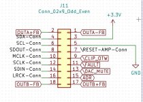
To give an idea of the interface to the controller, here is q picture of the connector in the current design.
Pins 1, 2, 17, 18 are I think not so important. Main signals are:
- I2S lines,
- I2C lines,
- /CLIP_OTW
- /FAULT
- /DAC_MUTE
- /RESET_AMP
- ADR
- controller would need an additional Analog input for Volume management (or inputs for a rotary encoder).
JMF
Pins 1, 2, 17, 18 are I think not so important. Main signals are:
- I2S lines,
- I2C lines,
- /CLIP_OTW
- /FAULT
- /DAC_MUTE
- /RESET_AMP
- ADR
- controller would need an additional Analog input for Volume management (or inputs for a rotary encoder).
JMF
Attachments
Tu push the idea forward, what would be the smallest/simplest uController to implement below features:
- support Arduino IDE
- ISP programming
- lowest is best
- I2C lines, possible to be master
- 2 Analog inputs at least (for volume and voltage monitoting)
- 5 Digital inputs at least (/CLIP_OTW, /FAULT, /DAC_MUTE, /RESET_AMP, ADR
- 3.3V power
Board could have the provision for such one (even if not systematically populated - good proposal from Doctormord)
I2S would be managed independantly.
(if no feedback here, I may post on ome Arduino forum)
Best regards,
JMF
- Home
- Amplifiers
- Class D
- [design log] Neat 2x170W I2S in, I2C controlled, integrated DSP amp (TAS3251)