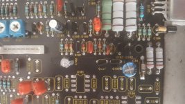
This is the area that is getting hot. (Q102,Q103,Q104,Q107, C34, the two 1W resistors)
Above post, I stated voltages on the zener diode, they were incorrect. Voltage on the 1n4744a 15V zener is 18 Vdc on the cathode and 0.000 on the anode.
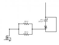
The voltage drop across the the two 200 ohm parallel resistors is 10 volts, 28 Vdc to 18 Vdc.
Above post, I stated voltages on the zener diode, they were incorrect. Voltage on the 1n4744a 15V zener is 18 Vdc on the cathode and 0.000 on the anode.
The voltage drop across the the two 200 ohm parallel resistors is 10 volts, 28 Vdc to 18 Vdc.
Attachments
Last edited:
I will remember that, thanks.
No, the hot transistors are in the "good" channel.
Yes, when I heated the group of transistors on the left channel the bias voltage dropped to 1.8mV. I could not focus the heat on a particular transistor, all I had was a hot air gun as a heat source, but could apply heat to the group of 5 transistors.
Last edited:
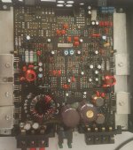
No, everything stays cool on the heatsink. Q104 is bent over towards the heatsink and it gets hot, but it is not clamped down in anyway.
I have a question about the zeners. They are reversed biased and being used as a voltage regulator, by design, being rated at 15 volts shouldn't the voltage across it be close to 15 volts if they are working properly, assuming input voltage is greater than breakdown voltage?
Thank you for your help.
You stated that the good channel was set at 1.3mv (assuming you mean that that's the voltage across the source resistors). Is that the lowest that it will go?
The Zeners have an internal resistance and that will make their voltage change with the current that's being driven through them. If the two 1k resistors are in parallel, you could lift one to see if the lower current would reduce the voltage across the Zeners. It's also possible that they have both drifted in value.
If you replaced the outputs in the bad channel, you may want to swap the outputs from one channel to the other. If the new FETs have a lower threshold and the bias circuit doesn't have enough range, that could be causing a problem.
Are you sure that the large source resistors are within tolerance? 8.9mv across them should be making the FETs heat up.
Yes, measuring across the source resistors. The good (R) channel was at 1.3 mV when I got the amp. I have not done anything to the right channel, since it was working I figured if I left it alone I could use that channel s my reference for the bad (L) channel.
The bias on the good channel will read 1.04mV when right pot turned fully C.C.
The two resistors are 200 ohm each and are in parallel relative to each other (not sure if I am explaining that correctly) and in series from the drain of the IRF540 and the cathode of the zener. They are new and read ~100 ohms in circuit.
I connected the preamp board and the voltage dropped to +/- 16.4 Vdc. I will try and lift one of the resistors to see if that changes anything.
I did have to change the output FETs as one was blown. I will try switching them and see what happens.
The 3W source resistors appear to be in tolerance they are 0.1 ohm and are new. When I got the amp one of the source resistor had lifted from the board. The previous person who attempted to work on the amp damaged the pads and vias and just had solder globbed on the lead of the resistor. They check okay as far as continuity across the traces (from lead to the components they connect to), but under current the connection may not be good. I will do some more tracing an attempt to connect them directly to where they are going with a piece of wire to test.
The FETs are remaining cool.
Today, I also changed the differential pair 2CS2362's, one MPSA56 which is laid over on the heat sink and one MPSA06 which was connected to one leg of the pot. The idle bias voltage is now 5.4 mVdc. For this channel all BJTs have been changed now.
I will swap the FETs tomorrow and post an update.
Attached is what I was trying to explain with regards to the regulator circuit.
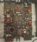
Do you think the 16volts is okay for the pre-amp board? I can see that in the past there has been a lot of heat in that area on both channels. The board is discolored under the resistors and the standoffs that help support the pre-amp board have some melting that has occurred.
I really appreciate your help, I realize the difficulty involved with trying to help over the internet with no circuit diagrams, not to mention dealing with someone new to electronics.
Attached is what I was trying to explain with regards to the regulator circuit.
Do you think the 16volts is okay for the pre-amp board? I can see that in the past there has been a lot of heat in that area on both channels. The board is discolored under the resistors and the standoffs that help support the pre-amp board have some melting that has occurred.
I really appreciate your help, I realize the difficulty involved with trying to help over the internet with no circuit diagrams, not to mention dealing with someone new to electronics.
Attachments
16v isn't excessive. If you replace the Zeners, that will tell you if it's normal for them to go that high or if it's likely due to the high current.
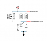
When drawing a diagram, the highest voltages are typically at the top of the diagram. The rail voltage is the source of the voltage to the resistors. The resistors allow the voltage to drop at the cathode of the Zener. The anode of the Zener is grounded. This is the positive regulator. The negative is similar but reversed (cathode of Zener is grounded), resistors connected to the negative rail.
When/if you need to draw other diagrams, include the circuit board designation and value for all components. It's also best to find software that allows you to draw on a grid and to make/use libraries of parts. That saves time and allows consistency.
The heat stress that you see is common for this type of shunt regulator.
Attachments
Do you have any spare resistor that would make that resistor slightly higher in value (either one to go in series with it or a resistor of slightly higher value?
If so, try making it slightly higher in value (set pot fully CCW) to see if that lowers the minimum bias current.
If so, try making it slightly higher in value (set pot fully CCW) to see if that lowers the minimum bias current.
- Status
- This old topic is closed. If you want to reopen this topic, contact a moderator using the "Report Post" button.
- Home
- General Interest
- Car Audio
- Phoenix Gold XS2300 Repair