I have an XS2300 BLK that I am attempting to repair. This will be my first repair so bear with me. This amp has had an attempted repair by someone else at some other time.
What I have found so far:
one output transistor is bad (STm IRF540)
one source resistor is the wrong resistance 1 ohm vs 0.1 ohm
one resistor is burnt so bad I can't see the markings but according to 1moreamp in another post it is 324 ohm 1/8w 1% which is connected "across the gate to source leads of the FET".
one MPSA56 PNP transistor case is broken.
I found the parts list from 1moreamp to rebuild the whole channel, so I am in the process of trying to order those parts.
I am having trouble finding the STmicro IRF540, so when looking for a comparable MOSFET from a different mfg. what are the important parameters to compare from the data sheets? It seems like I can match some but not all of the parameters from part number to part number.
Also for other parts it seems one supplier has one part and one might have another resistor other than Mouser, Digikey, what are some suppliers in the US that y'all have had luck procuring most of the parts from one place?
Thank you!
Perry,
I will give the phoenixphorum a try.
I came here for one, because I purchased the repair tutorial a while back, so I figured we would be speaking the same language since I was getting most of my knowledge from your work.
I also could tell 1moreamp was familiar with them, but he may not be active anymore since his last post was appears to be several years ago.
Thank you.
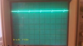
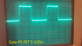
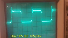
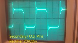
Could someone please look at these measurements and help me figure out what the spikes are at the first part of each wave?
These were taken on the power supply with the rectifiers removed. The external power supply was set to 12 Volts.
Should there be dc voltage on the center pad of where the rectifiers go? This particular amp has a black board that is two sided and shinning light through it and with my old eyes, I am having a tough time following the traces.
Attachments
-
 B+ to B-.jpg183.7 KB · Views: 63
 -
 Gate PS FET.jpg177.6 KB · Views: 65
 -
 Drain PS FET.jpg170.6 KB · Views: 61
 -
 O.S. Pins Rectifier.jpg188.6 KB · Views: 66
 -
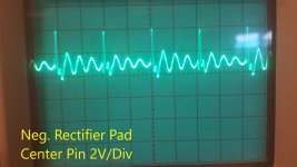 Neg. Rectifier Center Pin.jpg181.8 KB · Views: 64
 -
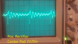 Pos. Rectifier Center Pin .jpg177.9 KB · Views: 25
 -
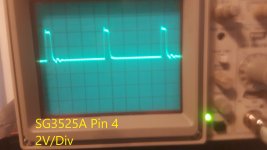 SG3525A Pin 4.jpg157.8 KB · Views: 23
 -
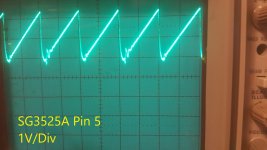 SG3525A Pin 5.jpg200.3 KB · Views: 27
 -
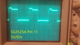 SG3525A Pin 11.jpg179.6 KB · Views: 29
 -
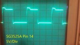 SG3525A Pin 14.jpg177 KB · Views: 26
The DC on the secondary is insignificant. If it matched the DC supply voltage, that could indicate that the transformer was shorted but that's not the case here.
The ringing on the rising edge of the drain waveforms isn't significant, at this point. This could change significantly after the rectifiers are reinstalled.
Is the gate waveform for all of the PS FETs (taken from the gate leg) identical for all of the PS FETs?
Some of the noise that you're getting is likely because you're relying on the scope ground to the 12v power supply ground. This generally works well enough and virtually the only thing I ever used but if you want to get better waveforms, you need to use the short scope probe ground lead. You must be VERY careful not to short the probe ground to adjacent pins.
For the PS gate waveform, you'd ground the probe to the source leg of the FET being tested.
For the driver IC waveforms, you'd ground to pin 12.
Perry,
Yes, on the PS FETs gate, the amplitude, pulse width and period are the same on all four FETS using the divisions of the scope to calculate. When using the DMM the difference in amplitude between two pairs is 0.19 Vdc.
The rail capacitors appear to be bulging at the tops. I ordered replacements but they are to tall, so I will have to reorder the correct ones. I could put the ones I have in for testing if that is suggested.
On the KA339 Comparator the only difference of the inputs and outputs is on the #3 comparator the + and - are reversed, (-) = 4.92V > (+) = 3.83 and output = .046 V. all other inputs were the reverse of this and outputs around 5 V each.
If the PS looks good for know, I will move on to the audio side. That is where the main problem still lies as the high current draw ~10amps at idle has stopped with the rectifiers removed. I think I will start pulling the zener and small signal diodes and checking them as well as replacing one resistor I found with much higher resistance than indicated by the markings , 1.8 Kohm vs 51 ohms respectively.
I have already replaced all of the A56 and A06 Transistors in the bad channel. There is one differential pair 2sc2389 that I have not replaced, but have a ~ equivalent part # to do so if necessary.
I will have to also do some studying on the proper testing of the op-amps, 4560D and NE5532.
To make sure I am understanding, when referring to the emitter resistors you are talking about the BJTs correct? If so by following the traces I found 5 resistor connected to the emitters of the MPSA56 and MPSA06 BJTs. They all have some dc voltage ranging from 0.02 to 1.2 Vdc. When comparing the "good channel" they also had Vdc on the corresponding resistors. I tested these with the current limiter in series with the B+.
With all the semis clamped down, the only thing on the board that is getting hot are the source resistors for the output FETs.
With all the semis clamped down, the only thing on the board that is getting hot are the source resistors for the output FETs.
I'm not sure. If I run the amp with only a 10 amp fuse on the B+ it seems "stable" the source resistors and output FETS get hot quickly. Both source resistors voltage is stable at ~ 0.235 Vdc.
When I place the headlamp in series the current draw drops from 10 amps to ~1.5 amps but you can see the lamp pulsating and the source resistors are fluctuating equally at 0.03 to 0.056 Vdc.
When I place the headlamp in series the current draw drops from 10 amps to ~1.5 amps but you can see the lamp pulsating and the source resistors are fluctuating equally at 0.03 to 0.056 Vdc.
Last edited:
In some amps, the bias pots are mirror image so one has to be fully clockwise to be at the minimum bias. Try turning the one in the defective channel clockwise to see if it will reduce the current draw.
Measure the voltage across the two orange diode pairs on the heatsink in the two channels to see if they're about the same.
Measure the voltage across the two orange diode pairs on the heatsink in the two channels to see if they're about the same.
Finally got back to this.
This revision of the board does not have the diode pairs clamped to the heat sink. I will try and get some decent pictures, I tried with my phone but due to the quality, they are useless.
I checked every diode in the bad channel by removing one lead from the board and they all checked ok, 0.6 to 0.75 V and open when reversed.
I did find one that I am not sure about that lies between the power supply and the output. It is D6 in the picture, a SF 24 "super fast rectifier diode" and the data sheet gives a Max Vf of 0.95V. This diode read forward 0.472 and open reversed. Is the forward voltage a problem?
So I changed both output FETS on the bad channel, found a few resistors that were toast or out of spec and changed them. Found three capacitors that were out of spec and or bulging changed them.
The amp will now play on both channels and things seem to be relatively even on both channel speaker outputs.
DC offset seems good 7mV and 5.5 mV
It is now drawing less than 1 amp at idle, whereas before it was drawing ~10 amps at idle.
Input at 12Vdc:
Rail/Secondary +28.1 Vdc and -27.4 Vdc
I think this is voltage for the differential pairs and bias circuit, on the cathode of SF-24 rectifier diode is 35.3 Vdc
On the bad channel I can not get the bias set any lower than 8.9 mV (pot full C.C.) it was more than 100 mV before I changed the components as listed above, whereas the good channel was set at 1.3 mV. I have removed one leg of all diodes from the pcb on the bad channel and the seemed okay.
The lower bipolar supply is high at 18 Vdc on both channels. I think it should be +/- 15 Vdc. The Vs max of the 4560D's is +/- 18 Vdc. Also the drivers, the 200 ohm 1W parallel resistors and one capacitor, which is one of the caps that were changed, get very hot at idle in this area on both channels. The Voltage on the anode of the 1N4744A 28Vdc and at the cathode is the 18Vdc going to the pre-amp board.
So I think my two main problems right now are the bias circuit/bias current and the voltage of the lower supply being to high.
Does anyone have any suggestions of where to go next?
Thank you.
Last edited:
- Status
- This old topic is closed. If you want to reopen this topic, contact a moderator using the "Report Post" button.
- Home
- General Interest
- Car Audio
- Phoenix Gold XS2300 Repair