I don't think the coupling capacitors I used have hurt the sound too much. I used either high current-type polypropylene or polycarbonate devices, basically whatever I could find from surplus sources or Ebay (I'm a cheapskate, in case you can't tell). A lot of the improvement I experienced with my current open loop design may well be because my old Nikko preamp had at least 5 electrolytic caps in the audio path, all of them about 25 years old... Having said that, I remember experiencing some resolution loss when I replaced my cranky homebrew preamp with the Nikko back around '81, so maybe it wasn't so hot even then, in spite of its impressive paper specs.
Having said that, the active design I'll be trying has fewer caps in the signal path, as I can use some feedback tricks for DC centering. I'm curious to hear if there is a difference.
This afternoon, I discovered another trick to squeeze some more juice out of the Pacific design, cutting distortion in half on both input and output stages, as well as improving the harmonic distribution when using a cascode at high signal levels. I like what I see in the simulations enough to move the single ended folded cascode design down a notch or two in the pecking order so I can try this idea sooner. Best of all, it allows me to ditch the 2SK170 and use all PN4393s. Long live the 4393! More on this later....
The thread that rises from the dead...
I'm waking this one up, as there is interest in some quarters in simple jfet open loop designs, and this is the first one that I did. It's basically the 2-fet Pacific design with cascode and added followers. It's hard to believe the design is 7 years old now.
Anyway, what I did was to take the original board from this thread (not documented all that well, so I'll draw and post a schematic later) and plot the gain-phase using an HP4194A gain-phase/impedance analyzer. The gain matching between channels was surprisingly good, even for this first effort.
Attachments
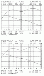
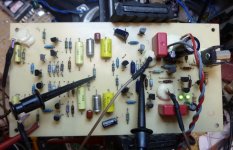
Here's a picture of the unit in question - doesn't look like much. The RIAA caps are a Wesco metalized PP (yellow) and a 33nF PP film/foil (silver) selected for 34 nF. The stubby yellow interstage coupling caps are Southern Electric (F-dyne) 1uF PC units, and the red output caps are 2.2 uF Wima MKS-4 PC. The yellow loading caps at the input are IMB polystyrenes. The on-board regulator is a discrete series pass circuit of my own design - I eventually changed to shunt regulators in later designs. The two green LEDs are the voltage reference for the regulator.
Attachments
Last edited:
Here's the thread that got me going, started only a few days after I joined Diyaudio in 2004 - http://www.diyaudio.com/forums/analogue-source/28223-ultrasimple-mm-mc-riaa-preamp-2-a.html .
I've gone through quite a few gyrations since then. One of my intentions when I round up all the boards is to do a photo-menagerie of stuff I've worked on, with links to the threads. That's one of the reasons I dredged up this old board and did the measurements.
I've gone through quite a few gyrations since then. One of my intentions when I round up all the boards is to do a photo-menagerie of stuff I've worked on, with links to the threads. That's one of the reasons I dredged up this old board and did the measurements.
Rising from death again!
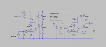
What do you think about this circuit?
It has nice gain and low distortion:
Fourier components of V(out)
DC component:-0.00435251
Harmonic Frequency Fourier Normalized Phase Normalized
Number [Hz] Component Component [degree] Phase [deg]
1 1.000e+03 5.272e-01 1.000e+00 -49.32° 0.00°
2 2.000e+03 1.399e-05 2.653e-05 -173.02° -123.69°
3 3.000e+03 6.353e-06 1.205e-05 -167.83° -118.51°
4 4.000e+03 3.297e-06 6.255e-06 -179.91° -130.58°
5 5.000e+03 2.640e-06 5.008e-06 -179.88° -130.55°
6 6.000e+03 2.200e-06 4.173e-06 -179.87° -130.55°
7 7.000e+03 1.886e-06 3.577e-06 -179.87° -130.54°
8 8.000e+03 1.650e-06 3.129e-06 -179.87° -130.55°
9 9.000e+03 1.466e-06 2.781e-06 -179.88° -130.56°
10 1.000e+04 1.319e-06 2.503e-06 -179.91° -130.58°
Total Harmonic Distortion: 0.003110%(0.003252%)
Here is the AC analysis:
And finally the noise analysis:
Do you think it is worth trying? Thanks!
What do you think about this circuit?
An externally hosted image should be here but it was not working when we last tested it.
It has nice gain and low distortion:
An externally hosted image should be here but it was not working when we last tested it.
An externally hosted image should be here but it was not working when we last tested it.
An externally hosted image should be here but it was not working when we last tested it.
Fourier components of V(out)
DC component:-0.00435251
Harmonic Frequency Fourier Normalized Phase Normalized
Number [Hz] Component Component [degree] Phase [deg]
1 1.000e+03 5.272e-01 1.000e+00 -49.32° 0.00°
2 2.000e+03 1.399e-05 2.653e-05 -173.02° -123.69°
3 3.000e+03 6.353e-06 1.205e-05 -167.83° -118.51°
4 4.000e+03 3.297e-06 6.255e-06 -179.91° -130.58°
5 5.000e+03 2.640e-06 5.008e-06 -179.88° -130.55°
6 6.000e+03 2.200e-06 4.173e-06 -179.87° -130.55°
7 7.000e+03 1.886e-06 3.577e-06 -179.87° -130.54°
8 8.000e+03 1.650e-06 3.129e-06 -179.87° -130.55°
9 9.000e+03 1.466e-06 2.781e-06 -179.88° -130.56°
10 1.000e+04 1.319e-06 2.503e-06 -179.91° -130.58°
Total Harmonic Distortion: 0.003110%(0.003252%)
Here is the AC analysis:
An externally hosted image should be here but it was not working when we last tested it.
And finally the noise analysis:
An externally hosted image should be here but it was not working when we last tested it.
Do you think it is worth trying? Thanks!
Last edited:
Well, you have a 40V supply with a 25V rated jfet, that would give me pause. A substantial negative signal at the preamp input might put the whole Vcc supply across the input jfet. Running the VCC at ~30V would help. I start with a 40V supply and knock it down to 30V with a shunt regulator.
Cascoding the input jfet is a good idea, especially if you plan on using an MM cartridge. Miller capacitance multiplied by the first stage gain might take the input loading capacitance beyond what is optimal for a given cartridge, when you add up the contribution of tonearm wiring plus cables plus input capacitance plus amplified Miller capacitance.
As far as RIAA cap values are concerned, you might have an easier time finding parts if you use 100nF and 34 nF (33nF + 1nF).
Hi wrenchone. I'm aware 40V is too much, and the actual simulations I run are 30V supply. The problem now is 2n5484 is no longer supplied by Mouser, RS, Farnell... My idea was to use some ready avalaible jfet, so 2n5485 is a possible alternative (or maybe 2n5457, 2n5458). Another solution could be smd jfets, like Toshiba 2sk880 (plus dip adapter). It's an audio low noise jfet, with nice gain. But it would be my first try with surface mount devices...
Thanks for your answer.
Thanks for your answer.
Well, the circuit works ok if the input signal is the average 5mV, but if it goes up to 50mV it begins to distort excessively due not enough headroom.
I have tried this alternative:
Better THD figures, less gain.
5mV input --> 400mV output, 0.041% THD
50mV input --> 4V output, 0.43% THD
150mV input --> 12V output, 1.18% THD
Quite nice for a discrete non-nfb circuit, but easily surpassed by a simple opamp circuit. I will keep experimenting (maybe an aikido topology, a nfb circuit?)
I have tried this alternative:
An externally hosted image should be here but it was not working when we last tested it.
imagenBetter THD figures, less gain.
5mV input --> 400mV output, 0.041% THD
50mV input --> 4V output, 0.43% THD
150mV input --> 12V output, 1.18% THD
Quite nice for a discrete non-nfb circuit, but easily surpassed by a simple opamp circuit. I will keep experimenting (maybe an aikido topology, a nfb circuit?)
Voltage overload seems to be the problem in this kind of non nfb circuits. They work quite well with the average output signal of a mm cartridge, but can be problematic with voltage peaks produced by cracks and pops, as they induce distortion.
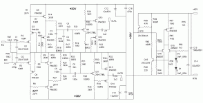
Tube phono preamps don't have this issue because of the high voltages they operate on. Why don't we try the same high voltages on solid stats designs? Well, jfets can't stand them. Maybe mosfets? Hey, why not? Let's experiment...
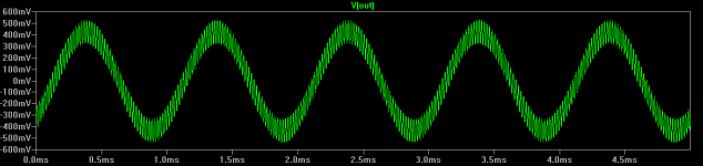
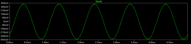
I've simulate this circuit using DN2540 depletion mode mosfets and 80V power supply:
dn2540 phono.png
As you can see I've put an AC voltage source in series with the DC source, to simulate power supply ripple. The 1uF caps that go from the DC voltage supply to the gate of the mosfets on the source followers after gain stages are there to inject power supply noise. That noise will null the noise brought by the gain stages (yes, it's just Broskie's Aikido technique). It works. Below you can see two transient analysis: without and with these caps.
dn2540 transient no caps.png
dn2540 transient aikido style.png
The circuit with the caps reject power supply noise way better.
The gain stages use cascoding to overpass the higher input capacitance of these mosfets, compared to jfets, and to bring gain up a little.
What about THD?
5mV input --> 450mV output (0,0125% THD)
50 mV input --> 4,5v output (0,15% THD)
100 mV --> 8,2V output (0,3% THD)
200mV input --> 18V output (0,6% THD)
300 mV input --> 25V output (1,47% THD)
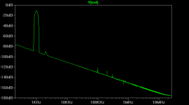
This is the THD plot with a 5mV input:
dn2540 THD.png
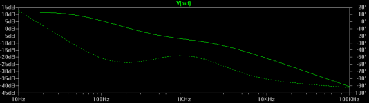
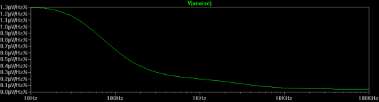
To complete the image, here are AC and noise analysis:
dn2540 ac analysis.png
dn2540 noise.png
Cons? You need a higher power supply, but not as high as in a tube preamp (and no heater supply either).
Tube phono preamps don't have this issue because of the high voltages they operate on. Why don't we try the same high voltages on solid stats designs? Well, jfets can't stand them. Maybe mosfets? Hey, why not? Let's experiment...
I've simulate this circuit using DN2540 depletion mode mosfets and 80V power supply:
dn2540 phono.png
As you can see I've put an AC voltage source in series with the DC source, to simulate power supply ripple. The 1uF caps that go from the DC voltage supply to the gate of the mosfets on the source followers after gain stages are there to inject power supply noise. That noise will null the noise brought by the gain stages (yes, it's just Broskie's Aikido technique). It works. Below you can see two transient analysis: without and with these caps.
dn2540 transient no caps.png
dn2540 transient aikido style.png
The circuit with the caps reject power supply noise way better.
The gain stages use cascoding to overpass the higher input capacitance of these mosfets, compared to jfets, and to bring gain up a little.
What about THD?
5mV input --> 450mV output (0,0125% THD)
50 mV input --> 4,5v output (0,15% THD)
100 mV --> 8,2V output (0,3% THD)
200mV input --> 18V output (0,6% THD)
300 mV input --> 25V output (1,47% THD)
This is the THD plot with a 5mV input:
dn2540 THD.png
To complete the image, here are AC and noise analysis:
dn2540 ac analysis.png
dn2540 noise.png
Cons? You need a higher power supply, but not as high as in a tube preamp (and no heater supply either).
Attachments
Last edited:
I generally relegate the DN2540 and siblings to current source duty because of the high input capacitance, which may make it impossible to properly load an MM cartridge. Infineon has some surface mount depletion mode mosfets with lower capacitance. The LND150 also has much lower capacitance, but at the cost of much lower IDSS and transconductance.
I don't worry about ticks an pops introducing distortion, as an open loop circuit should handle overload relatively gracefully, unlike a feedback-based amp, which may temporarily go crazy during clipping events.
I don't worry about ticks an pops introducing distortion, as an open loop circuit should handle overload relatively gracefully, unlike a feedback-based amp, which may temporarily go crazy during clipping events.
- Status
- This old topic is closed. If you want to reopen this topic, contact a moderator using the "Report Post" button.
- Home
- Source & Line
- Analogue Source
- Open Loop Follies, Pt. 1