Werner said:
I don't think you want 25V over the input FET with 8mA through it. At 200mW it will run hot.
Watch out for excess gate current due to impact ionization on those n-channel Toshiba FETs at high Vds. The p-channel ones don't have it due to the mobility difference. Toshiba matched the gm at Id on the complementary devices but the other properties (such as cgs/cgd) are sometimes very different.
n-channel gate leakage
This is a big deal in transformer coupled circuits (and some others, too), which is why I tend to use p-FETs as input devices. And it doesn't tend to show up on many spec sheets. When I've seen curves of gate leakage versus Vds or Vdg, they look very nonlinear, sort of stepping up to a high value pretty suddenly at a certain voltage. In the absence of good, complete data sheets, is there a way to predict this voltage so that it can be dealt with in a design?
This is a big deal in transformer coupled circuits (and some others, too), which is why I tend to use p-FETs as input devices. And it doesn't tend to show up on many spec sheets. When I've seen curves of gate leakage versus Vds or Vdg, they look very nonlinear, sort of stepping up to a high value pretty suddenly at a certain voltage. In the absence of good, complete data sheets, is there a way to predict this voltage so that it can be dealt with in a design?
Unfortunately no, it has to do with the grading of the field where pinch off occurs. Short channels are worse so high gm FET's suffer more. The gradient gets to be thousands of a volt per meter and the electrons get wacked right out the gate.
a single ended preamp with active feedback will work with everything that is hanging off the base/gate/grid, including the cartridge. This makes a case for using a diff pair to separate the feedback network from the cartridge.
I simulated 2 versions of simple RIAA active feedback preamps with cascoded JFET inputs, one single-ended, one differential. These have Avol of 50dB and feedback network is set for 27dB gain at 1kHz, too low for normal use but easy to calculate for +/- 1dB RIAA accuracy. I checked the AC input impedance magnitude by AC analysis, applying RIAA input, 7.5mV @ 1kHz. At 1kHz se was 552Meg, diff was 498Meg, at 15kHz se was 149Meg, diff was 159Meg. So at least by simulation in these simple cases, there is no significant difference in AC input impedance with frequency, and I can't see how cartridge interaction would be different.
This is the single ended version:
Attachments
Nuvistor - There was a definite justification Holman used for preferring a differential input stage over single ended with active feedback. I'd have to search my old papers to find it. This could take a long while, as I moved not too long ago, and I have no real idea where to start looking. Meanwhile, you go your way, and I'll go mine... This did start as a discussion of an open loop design, anyway.
Werner - I don't really care if a circuit was designed by John Curl or Nelson Pass or JHC Himself - if you don't question and analyze, you won't learn anything. They're just circuits, not holy writ from on high. With that in mind, several points.
Models - I'm using the models provided by Orcad for my simulations. Fortunately, they have several libraries of Japanese and European devices, including the 2SJ74 and 2SK170. I haven't checked for the 2SK389. The 2SK170 model seems about equivalent to a BL ranking.
Power dissipation - true, 200mW dissipation will bring a TO-92 transistor to around 100C at room ambient. However, simulations don't get hot, and there are ways around the problem. First would be to use a lower ranking FET that would have a lower idle current for the same VGS. The model Orcad uses for the PN4393 is middle of the road, probably 20-odd ma IDSS. Since the IDSS spread for the PN4393 goes all the way down to 5ma, there is plenty of room for selection of a lower IDSS device. I also tried manipulating resistor values to get a lower idle currrent, yet retain the same stage gain. I was able to get the idle current down to about 5ma. With this idle current, the harmonic structure after simulation is almost exactly the same as with the higher idle current. However, there is a better way to solve the thermal problem and several others - read on....
VGS and impact ionization - If you can get a full data sheet or a family specification for a JFET, there will be a curve for gate leakage current vs VDS. This curve is fairly flat for lower values of VDS. For higher voltages, there is an inflection point, then the gate leakage starts to rise eponentially with VDS. The voltage for this inflection point depends on FET design. For the PN4393, it's about 15V, which turns out to be pretty high compared to other FETS. The 2SK170 data sheet does not even bother to show the flat portion of the gate leakage curve. The leakage is already in the exponential region at 8V VDS. This is not too surprising, given the large gate area required to get such a low noise device.
The Siliconix FET application manual advises one to bias a JFET in the flat region of the gate leakage curve if low drain leakage is of paramount importance. No doubt this also releives any concern about impact ionization. Operating in the lower portions of the exponential region probably wouldn't be a big disaster. I imagine that just about every non-cascoded 2SJ170 design out in the world is operating this way. It would probably take some advice from a very seasoned and savvy JFET apps engineer to determine just where impact ionization will start to be a problem. Maybe I'll try giving Siliconix/Vishay a call - they're about ten miles down the road from where I work. At any rate, there's a simple solution to fix this problem for the most part, at least regarding the SE folded cascode circuit originally cited by Werner - read on...
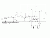
Solutions - As an engineer, I was bothered by the poor ripple rejection of the original resistor loaded folded cascode circuit cited by Werner, but also apalled by the harmonic structure of the first current source loaded solution that I simulated. I went back to the current source loaded circuit and substituted a perfect current source for the original transistor current source. I was expecting worse simulation results, but instead, the harmonic structure turned out to be as good or better than the resistive solution, with 0.005 % THD, all second harmonic.
Substituting a p-channel JFET current source for the perfect current source is almost as good. In this case, I used a J175 p-channel FET, which is normally used as an analog switch, but can be operated successfully in the linear region, just like the PN4393. This left the problems of gate leakage/impact ionization and power dissipation in the input PN4393.
The solution for both these problems is to split the power supply from a single +30V power supply into a +/- 15V supply. The input JFET and current source FET are operated from the +15V supply to ground, The rest of the circuit is operated between the +/- 15V rails. The cascode transistor works admirably as a level shifter. The PN4393 now operates at a much lower VDS, solving both the power dissipation and gate leakage/impact ionization problem. The simulation shows just a touch more 3rd harmonic distortion as a result of this change, but all the higher order harmonics are way down in the mud, and the THD is still atound 0.005%. This is pretty good for an open loop design. As usual, the challenge will be to see whether the circuit measures as well as it simulates.
The circuit I simulated is shown in the attached figure. I could work a little harder and get better output voltage centering and reduce the idle current, but I didn't bother for now. I think it is also possible to use a bipolar current source and get about the same results, and I think I know how. This is left as an exercise for the curious.
I started this whole exercise to try and find out several things for myself:
1) Is there any audible difference (using my 51 year old ears) between a good open loop design and a good closed loop design?
2) Does a good Orcad simulation of a circuit come close to predicting what will happen with actual measurements, especially with regard to THD and harmonic structure?
3) Can I tell the difference between a design with a "good" harmonic structure and one with a "bad" harmonic structure?
With this in mind, I have 5 power amplifier designs and two preamp designs scattered across my work bench awaiting assembly. They were chosen for their "good" harmonic structures in simulations. The design I reported here happens to be the first to see daylight.
I am extremely happy so far with the line amplifier portion of the preamp (even though nobody has paid any attention whatsoever to that bit). The direction this thread has taken has suggested some possible circuit changes that may be even better.
There are some possible incremental improvements for the "Pacific" open loop RIAA portion of the preamp, the first being to add a cascode FET to the first stage. Any other changes would require a complete re-layout and rebuild, and I will leave them for later. I want to try comparisons with a closed loop passive RIAA preamp first.
So far, questions 1) and 3) are still undecided for me, while 2) is a qualified yes, with one data point. Obviously, I will need to do a lot more building and testing and listening.
If I can get the single ended folded cascode circuit to operate at a gain of less than 10, it will be a good candidate for testing questions 2) and 3), as I can then build a line amp to substitute for the one I'm currently using. It will be interesting to see if the original current loaded implementation will test as having a harmonic structure as horrible as the simulation. If so, will I be able to tell the difference in my system? The same goes for the improved version of the circuit.
Werner - I don't really care if a circuit was designed by John Curl or Nelson Pass or JHC Himself - if you don't question and analyze, you won't learn anything. They're just circuits, not holy writ from on high. With that in mind, several points.
Models - I'm using the models provided by Orcad for my simulations. Fortunately, they have several libraries of Japanese and European devices, including the 2SJ74 and 2SK170. I haven't checked for the 2SK389. The 2SK170 model seems about equivalent to a BL ranking.
Power dissipation - true, 200mW dissipation will bring a TO-92 transistor to around 100C at room ambient. However, simulations don't get hot, and there are ways around the problem. First would be to use a lower ranking FET that would have a lower idle current for the same VGS. The model Orcad uses for the PN4393 is middle of the road, probably 20-odd ma IDSS. Since the IDSS spread for the PN4393 goes all the way down to 5ma, there is plenty of room for selection of a lower IDSS device. I also tried manipulating resistor values to get a lower idle currrent, yet retain the same stage gain. I was able to get the idle current down to about 5ma. With this idle current, the harmonic structure after simulation is almost exactly the same as with the higher idle current. However, there is a better way to solve the thermal problem and several others - read on....
VGS and impact ionization - If you can get a full data sheet or a family specification for a JFET, there will be a curve for gate leakage current vs VDS. This curve is fairly flat for lower values of VDS. For higher voltages, there is an inflection point, then the gate leakage starts to rise eponentially with VDS. The voltage for this inflection point depends on FET design. For the PN4393, it's about 15V, which turns out to be pretty high compared to other FETS. The 2SK170 data sheet does not even bother to show the flat portion of the gate leakage curve. The leakage is already in the exponential region at 8V VDS. This is not too surprising, given the large gate area required to get such a low noise device.
The Siliconix FET application manual advises one to bias a JFET in the flat region of the gate leakage curve if low drain leakage is of paramount importance. No doubt this also releives any concern about impact ionization. Operating in the lower portions of the exponential region probably wouldn't be a big disaster. I imagine that just about every non-cascoded 2SJ170 design out in the world is operating this way. It would probably take some advice from a very seasoned and savvy JFET apps engineer to determine just where impact ionization will start to be a problem. Maybe I'll try giving Siliconix/Vishay a call - they're about ten miles down the road from where I work. At any rate, there's a simple solution to fix this problem for the most part, at least regarding the SE folded cascode circuit originally cited by Werner - read on...
Solutions - As an engineer, I was bothered by the poor ripple rejection of the original resistor loaded folded cascode circuit cited by Werner, but also apalled by the harmonic structure of the first current source loaded solution that I simulated. I went back to the current source loaded circuit and substituted a perfect current source for the original transistor current source. I was expecting worse simulation results, but instead, the harmonic structure turned out to be as good or better than the resistive solution, with 0.005 % THD, all second harmonic.
Substituting a p-channel JFET current source for the perfect current source is almost as good. In this case, I used a J175 p-channel FET, which is normally used as an analog switch, but can be operated successfully in the linear region, just like the PN4393. This left the problems of gate leakage/impact ionization and power dissipation in the input PN4393.
The solution for both these problems is to split the power supply from a single +30V power supply into a +/- 15V supply. The input JFET and current source FET are operated from the +15V supply to ground, The rest of the circuit is operated between the +/- 15V rails. The cascode transistor works admirably as a level shifter. The PN4393 now operates at a much lower VDS, solving both the power dissipation and gate leakage/impact ionization problem. The simulation shows just a touch more 3rd harmonic distortion as a result of this change, but all the higher order harmonics are way down in the mud, and the THD is still atound 0.005%. This is pretty good for an open loop design. As usual, the challenge will be to see whether the circuit measures as well as it simulates.
The circuit I simulated is shown in the attached figure. I could work a little harder and get better output voltage centering and reduce the idle current, but I didn't bother for now. I think it is also possible to use a bipolar current source and get about the same results, and I think I know how. This is left as an exercise for the curious.
I started this whole exercise to try and find out several things for myself:
1) Is there any audible difference (using my 51 year old ears) between a good open loop design and a good closed loop design?
2) Does a good Orcad simulation of a circuit come close to predicting what will happen with actual measurements, especially with regard to THD and harmonic structure?
3) Can I tell the difference between a design with a "good" harmonic structure and one with a "bad" harmonic structure?
With this in mind, I have 5 power amplifier designs and two preamp designs scattered across my work bench awaiting assembly. They were chosen for their "good" harmonic structures in simulations. The design I reported here happens to be the first to see daylight.
I am extremely happy so far with the line amplifier portion of the preamp (even though nobody has paid any attention whatsoever to that bit). The direction this thread has taken has suggested some possible circuit changes that may be even better.
There are some possible incremental improvements for the "Pacific" open loop RIAA portion of the preamp, the first being to add a cascode FET to the first stage. Any other changes would require a complete re-layout and rebuild, and I will leave them for later. I want to try comparisons with a closed loop passive RIAA preamp first.
So far, questions 1) and 3) are still undecided for me, while 2) is a qualified yes, with one data point. Obviously, I will need to do a lot more building and testing and listening.
If I can get the single ended folded cascode circuit to operate at a gain of less than 10, it will be a good candidate for testing questions 2) and 3), as I can then build a line amp to substitute for the one I'm currently using. It will be interesting to see if the original current loaded implementation will test as having a harmonic structure as horrible as the simulation. If so, will I be able to tell the difference in my system? The same goes for the improved version of the circuit.
Attachments
Hi wrenchone -
Thanks for starting this engaging thread, it's been a while since I've seen this kind of discussion in the Analogue forum.
Have you considered cascoding J1 and J5 with high Vp JFETs in addition to the folded cascode? I used MPF4392 in my RIAA schematics for this. I think this would solve your J1 Vds problem and increase J5 ro, and you wouldn't need two supplies to help with J1 Vds.
Yep, that's why I've been making my points about active feedback at the risk of thread hijacking, and questioning the Holman hypothesis. I still don't see where it applies to series feedback due to isolation of the feedback summing node from the input by the input tube/transistor, though I can see where it applies to shunt feedback with low feedback, where the feedback summing node is directly connected to the base/gate/grid. Hopefully you'll find your papers and let us know about them.
Are you working on a good closed loop design or are you referring to your Nikko?
Your schematic in post 1 shows a buffer with cascaded followers, first is simple current source loaded, second is JFET version of White follower. Your later posts of RIAA preamps use simple buffers after the second gain stage. What are you using now? Perhaps the lack of attention to the line portion is because there have been threads on open loop buffers in the Solid State and Chip Amp forums, or because low-level amplifiers challenge the limits of devices and designs more than line-level. I haven't seen much in these forums on discrete line amplifiers with gain, though.
Thanks for starting this engaging thread, it's been a while since I've seen this kind of discussion in the Analogue forum.
Have you considered cascoding J1 and J5 with high Vp JFETs in addition to the folded cascode? I used MPF4392 in my RIAA schematics for this. I think this would solve your J1 Vds problem and increase J5 ro, and you wouldn't need two supplies to help with J1 Vds.
if you don't question and analyze, you won't learn anything
Yep, that's why I've been making my points about active feedback at the risk of thread hijacking, and questioning the Holman hypothesis. I still don't see where it applies to series feedback due to isolation of the feedback summing node from the input by the input tube/transistor, though I can see where it applies to shunt feedback with low feedback, where the feedback summing node is directly connected to the base/gate/grid. Hopefully you'll find your papers and let us know about them.
Is there any audible difference (using my 51 year old ears) between a good open loop design and a good closed loop design?
Are you working on a good closed loop design or are you referring to your Nikko?
I am extremely happy so far with the line amplifier portion of the preamp (even though nobody has paid any attention whatsoever to that bit).
Your schematic in post 1 shows a buffer with cascaded followers, first is simple current source loaded, second is JFET version of White follower. Your later posts of RIAA preamps use simple buffers after the second gain stage. What are you using now? Perhaps the lack of attention to the line portion is because there have been threads on open loop buffers in the Solid State and Chip Amp forums, or because low-level amplifiers challenge the limits of devices and designs more than line-level. I haven't seen much in these forums on discrete line amplifiers with gain, though.
Nuvistor -
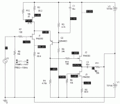
The next in line for incorporation and testing in my preamp box is a closed loop folded cascode design. The inputs are your classic diff pair using matched 2SK170s, essentially a discrete opamp. The RIAA section of the preamp uses two of these opamps with passive equalization in between. The lineamp is a pair of the same discrete opamps configured for a gain of +5.
After the results I've seen so far with the first setup, the Nikko is relegated to the shelf as far as I'm concerned. When I get the closed loop stuff in place, it will be the subject of a second thread, though I'll probably end up referencing this one. I might do a third set of tests using the folded cascode design when I figure out how to optimally use it.
I tried doing some extra cascoding with the folded cascode as you mentioned. but the results weren't worth it (it didn't do anything exciting). The input transistor is already cascoded, and adding a cascode to the current source FET eats up valuable voltage margin. It looks like the key to decent harmonic distribution with this design may be maintaining an adequate voltage across the current source. I proved this by doing a different sort of bipolar current source that minimized the voltage across its emitter resistor, and got a decent harmonic spread.
I just now finished simulating a gain of 5 version of the single ended folded cascode circuit for use as a line amp. Distortion figures are not near as good as those for the follower circuit. I get a THD of about 0.5% at 200mV excitation level, 10kHz. The harmonic distribution is ok, though. A "lower" quality of FET in the input stage actually seems to work better than a classy device like the 2SK170. I ended up using a PN4303 as an input device in the simulation, as I happened to buy a bunch of these from Electronic Goldmine, and they have decent (though not spectacular) gain and noise figures. The humble 2N5457 actually does reasonably decently as an input device in this application.
One of the incentives for continuing with the folded cascode circuit would be to show that it doesn't take an exotic Japanese device to get excellent results in an RIAA amplifier. The PN4393 will have a higher noise figure than the 2SK170, but I suspect that it won't be an issue at all for a MM or MI preamp. The folded cascode circuit also seems to really shine for low input applications. Really, <0.01% distortion for an open loop design is not to be sneezed at....
The Fairchild PN4393 is only $0.13 in 100piece quantities from Mouser, or about $0.38 if you insist on the Siliconix/Vishay device. I would go for the Vishay device, as it has a higher breakdown voltage spec (40V vs 30V), and is more completely specified in the data sheet. Since this device is really too cheap to counterfeit, you are pretty certain to get what you ordered. Long live the 4393!
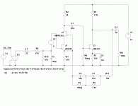
To be really clear about what I'm doing, the current preamp I'm running uses a modified "Pacific" architecture for the RIAA preamp. The gain cell consists of a simple common source amplifier with a current souce loaded source follower. This gain cell is the left-hand circuit shown in my first post. The RIAA preamp is two of these cells with a passive RIAA network in between The complete RIAA schematic is shown in a later post in this thread.
The line amp portion of the preamp consists of two cascaded source followers with current source loading. This circuit is shown in the first post.
The RIAA and line amp portions are each on separate cards with dedicated discrete voltage regulators using a pair of green LEDs as a reference. These regulators knock down a 40V unregulated DC source to 30V. The unregulated supply is in a separate box, and uses a 28-0-28V toroidal transformer with 6800uF filters for each supply. I configured the supply for +/- 40V outputs for flexibility, though I'm only using the +40V supply at present. Rectifiers are BYV28-150 ultrafast diodes with a ferrite bead in series with each rectifier and a 0.1uF + 4.7 ohm snubber across the bridge. There is a canned EMI filter at the AC input to the supply, and a ferrite common mode filter at the output.
Adding extra cascoding to the input transistor in your folded cascode stage would primarly reduce its Vgs/Vdg and gate current, drain voltage is already clamped. Nat Semi at one time had monolithic dual cascoded JFETS with the low Ig vs. Vdg prominently pointed out in the datasheet. Adding extra cascoding to the current source is probably "gilding the lily". Certainly adding extra cascoding reduces supply voltage margin, +15V would be barely enough.
Since you will soon have both open and closed loop gain stages, you could try a passive RIAA with an open-loop single-ended first stage and closed-loop second stage, first stage noise may be better with single-ended, and the closed loop second stage could take higher input levels with lower distortion than an open loop stage.
By coincidence, I've been simulating discrete transistor gain stages for headphone amplifiers, and the classic "Lin" topology with resistive-loaded differential input and single-ended current source loaded second stage can have low distortion, less than 0.005% with non-inverting gain of 3, input is U406 cascoded with MPF4392, with Jung's version of the LH0002 diamond buffer into a 32 ohm load. Avol is about 60dB and stability compensation is needed, 1kHz dominant pole.
Having used the 2N5457 in the front end of phono stages, I can say that it works better than you might expect. I don't have the schematic at hand, but I believe it was configured as a common Source with resistive loading for the first stage. Vds=15V, perhaps? Can't remember. Second was a follower biased by an equal value resistor, thus making use of the "pre-distortion" trick. Given that the 2N5457 won't carry much current, it would not work well with a low impedance load, but in this application the next stage would generally have a known Zin and that shouldn't be a problem.
I remember playing with a normal cascode (i.e. not folded) on the bench, but can't remember listening to it. At this point in time, I can't remember why I backed away from that configuration.
Granted, the 2SK170 is a lower noise device and is capable of higher gain, but it's also harder to get, more expensive, and you never know whether you're going to get GR, BL, or VI devices. All I've been able to lay hands on are GR, and it's always a mystery until you open the box as to what you're getting. The 2N5457 is easy to get and cheap. It's no better, current-wise, than the GR devices, but at least you know what you're getting going in. I don't know that I'd go so far as to call it a 'sleeper' part, but it does seem to get the job done, on time and under budget.
For what it's worth, I have gradually drifted towards passive RIAA for sonic reasons, not theoretical. Presumably phase shift and other such feedback-related nuisances are involved, but given that people tend to react as though stuck with a pin if you criticize feedback, I prefer to avoid such discussions. There've been enough arguments about open loop vs. feedback designs elsewhere. I'm not trying to start another here.
Grey
Nuvistor -
using a sigle 30V supply, cascoding would reduce the voltage on the input FET, but I got the same result just by moving the supplies around. Philosophically speaking, I don't like to double cascode a stage, though I have done it at times with folded cascode power amps when the supply voltages are really high.
G Rollins - Yeah, the 2N5457 ain't all that bad, though the 5459 gives you a little more current capability to play with. The only big disvantage I can see with the device family is the relatively low specified breakdown voltage (25V). However, the gate leakage vs. VDS curve doesn't kink upward until 20V or so (at least for the Siliconix devices), which is really nice. The gain is relatively low, too, but this may be just what is needed for some applications. I made a stab last year at making a JFET based SRPP preamp, but centering the output voltage was a big problem with the JFETs I was using, as there was just too much gain. I may try it again using all 2N5457 or 2N5459.
As far as the 2SK170s are concerned, I got mine from MCM. I made a point of it to email them first and ask what was in stock before I ordered, then got enough pieces so that I wouldn't need to reorder for a while. They (MCM) haven't lied to me yet, and having a bunch of pieces on hand makes matching easier.
You've had more luck than I have. If I ask whether they (MCM, CEITRON, et. al.) have GR, BL, or VI in stock, they act as though I'm making the worst sort of imposition. I buy as many as I can justify and sort by Idss. Still, if all they have available is GR, and you want BL, you're stuck. I have yet to run across a circumstance where someone comes back to the phone and cheerfully announces that they have all three grades in stock and which kind did I want...
With, say, the Siliconix J310s, you can go to Mouser and see what they've got right then, with no hassle involved. I managed to get some 2SK389 & 2SJ109 BL, but everything else has always been GR. The only VI I have on hand were given to me; I've never come across any for sale.
I once called Toshiba USA to see if I could work things from the top down. They told me that the 2SK389 didn't exist, which I found to be a rather curious statement. I fail to see why Toshiba doesn't want to sell the parts here in the US. All the parts seem to flow through shadow channels, rather than being supported officially. Generally speaking, if there's demand and you have product, you make at least a token effort to sell your product. There is a reason, I'm sure, for Toshiba's position, but I haven't discovered it yet.
Grey
I think the folks at Toshiba USA are familiar only with the digital side of the business. If you're not asking about RAM or MPUs, it's terra incognita to them. Nobody here but the fanatics like us know about the discretes.
Grey -
I have seen little discussion of open loop vs. feedback designs related to phono preamps, most has been about power amps.
This post by jcarr is about all I have been able to find on the subject.
I have been inclined to start a thread on comparison of active and passive RIAA but doubt that it would be taken seriously in these forums, for the reason you give.
wrenchone said:
The solution for both these problems is to split the power supply from a single +30V power supply into a +/- 15V supply. The input JFET and current source FET are operated from the +15V supply to ground, The rest of the circuit is operated between the +/- 15V rails.
Similar to the folded-cascode MC input of Commuteman, see bottom of thread, and also to the Pink Triangle PIP II, although that one had a differential FC input.
http://www.diyaudio.com/forums/showthread.php?s=&threadid=36260&perpage=10&pagenumber=2
Well, Werner, it just goes to show that there's nothing truly unique in this world any more. If I go ahead and try the SE folded cascode approach (I'm tempted), I'll probably use something besides an op amp for the second stage, though. It's all academic at this point, as this project will be at least several slots away from the head of the line. I want to try cascoding the front end of my modified Pacific first (it's easy, as the places for cascode FETs are already on the board), then bring up my closed loop folded cascode preamp, as those boards are all stuffed and ready to go.
I also have several power amps that need to be fitted with heat sinks and cases. Since the amp I'm currently using is a modified Leach design built in 1979 out of stuff at hand, I'm curious to hear the effect of changing the power amp to a more modern (and may I say, better constructed) design.
I also have several power amps that need to be fitted with heat sinks and cases. Since the amp I'm currently using is a modified Leach design built in 1979 out of stuff at hand, I'm curious to hear the effect of changing the power amp to a more modern (and may I say, better constructed) design.
My objections to active RIAA EQ are similar to those for high NFB in other circuits. Loss of detail and air, coupled with a tendency for "sparkle" in the upper frequencies that some people seem to enjoy though it isn't the way real music sounds. I have heard feedback EQ circuits that don't have that overly etched high end, but the detail retrieval problem seems universal, differing only in degree.
I'm not saying that feedback EQ is the kiss of death. It isn't. There are some fine sounding units out there using that strategy. It's just that passive EQ seems to sidestep the problem entirely, so why tempt fate?
I came to solid state from tubes. The ability to build a tube circuit with a knob on the front that controls the NFB is luxury beyond compare when you want to listen to the effects of feedback on reproduction quality. It doesn't take long to grow suspicious of high rates of feedback (tube stuff rarely goes over 15-20dB NFB--more normally 10-12dB on the better gear). This led me to the idea of circuits that are wide bandwidth when run open loop. Not because of TIM, etc. but simply so that I didn't have to push a 5kHz top end out to 100kHz by using gobs of feedback. I discovered that it sounded better. If the TIM and so forth is lower, then so much the better. Since active RIAA, by definition, includes a great deal of feedback at the upper frequencies I started paying more attention to passive EQ ideas.
No, I haven't built equivalent active and passive EQ circuits and compared them, in part because I would design such circuits differently from the ground up. I suppose the easiest way to go about such a task would be to take an opamp like an AD797 and put active and passive EQ around it. It's a low priority with me.
I've been working on a phono stage recently, though my time has been badly fragmented. I'm about two-thirds done and am tempted to pack my things and go to a desert island where there are no telephones so as to fiddle undisturbed. With that in mind, this thread comes at an opportune time. There are similarities and differences between my circuit and wrenchone's and I'll be watching with interest.
Grey
Hi Grey -
My, I did not expect this response, thanks for your consideration.
I haven't been much for phono upgrading over the years, I still use Shure V15VMR on a Thorens TD125 with original Infinity Black Widow, yeah MM doesn't have the extended treble of MC but I really like the midrange, and the Shure + Widow is easy on the grooves. My phono pre for about 10 years was 2 op amps with passive RIAA network between them and DC servo, most recently OPA627 and LM6171 with class A output biasing, LM317 regs, R+1n,100n,10u C bypass on each OPA +/-. Reasonably low noise, clean, but kinda bland sounding. I have an Onkyo P304, it must be high Avol active EQ, solid bass and dynamic, noisefree for MM but low-level midrange and treble detail are badly shredded like early CDs. I tried various Dyna PAS3 tweaks, cascoded 6072 was the best, maybe a little more tuneful in the midrange and more soundstage depth but dull treble.
I had heard about passive RIAA having the best sonics but wondered why Pass Xono was active. I looked at AR tube phono schematics and was intimidated by their byzantine complexity. I liked the PAS3's richness and wanted to try tubes but was concerned about 2nd stage noise which is attenuated by 1st stage in active RIAA. I ended up trying active around 2 single-ended gain stages, series feedback to 1st stage cathode, JFET mu follower loads and 5755 triodes, and found midrange depth and detail I had never heard before. With the Lipshitz formulas in Mathcad I could calculate EQ and Spice sim to final trim, getting +/-0.1dB against an inverse RIAA on the bench from Spice sim values on the first try, the Shure isn't better than +/-0.5 anyway, and the now fashionable 50kHz zero is a neat solution to the closed loop gain rolloff problem. The simulated circuit has Avol of 75dB to 20kHz, 72dB at 32kHz, and Acl of 42dB at 1kHz. The main problems were dealing with the JFETs dying when I probed around with power up and loop comp, 2-pole comp around 2nd stage worked the best, earlier versions sounded grainy and dull. Low output impedance allowed a low impedance feedback network and a 100 ohm first stage cathode resistor (!), the 5755s allow 150mV Vgk with no grid current at 135 Vp. I haven't measured S/N but it's quieter than the best records I have with MM, plenty of 1/f noise from the cascoded PN4302 JFETs, 2SK117s are quiet but I don't want to blow up too many of those. No problems with overload margin.
I agree with you that it's best to design for passive or active from the ground up, instead of configuring a specific circuit for either passive or active. All-passive needs 2 30x gain stages either by low gm*(Rl//rp) or by feedback, HK Citation I is an example of the latter. Single loop active needs high Avol for good EQ, preferably with an open loop pole above 20kHz. Hybrid like Werner's are another option since 2nd stage Avol and feedback can be less than for all-active and first stage can be open-loop, you can even try a tube 1st stage and SS 2nd stage. I'd like build a "classic" discrete passive RIAA for a fair hearing, I have the parts for a 6ER5/6GK5 tube or cascoded/buffered 2SK117 JFET version where I can try resistive loading, which I didn't want to do with my active. I'd also like to build a hybrid, somewhat like Werner's or wrenchone's latest. Hopefully my hearing acuity will still be OK by the time I'm done, I seem to have the time to do about one of these each year.
One of the things I find interesting about wrenchone's circuit it that it is cap-coupled at the output. This is something that I've been experimenting with recently. My reasoning is that the problems introduced by a capacitor are going to be less than those introduced by a level shifter and the necessary feedback to lock the output to DC.
This is heresy in solid state, but the norm in tubes. It's an interesting option to play with.
I tried a complementary differential in the John Curl mode, but the phase-splitting wasn't sufficient for my needs. (I'm building a balanced circuit. Ideally, I'd like to be able to have the option of putting in either a balanced or an unbalanced signal and having it balanced at the output.) The plus side was that the circuit could be adjusted to have very little DC offset. I worked at it for a while, set it aside, then went back to it again before deciding to go with a single 2SK389 since it offered a good balanced output.
Grey
- Status
- Not open for further replies.
- Home
- Source & Line
- Analogue Source
- Open Loop Follies, Pt. 1