spladski, I tried using the capacitor offset method as you did and THD is still 0.0031%. It seems the problem is Q3, I think it conducts somehow, I added C3 so in the off state we only shunt the AC component to ground. It lowered the THD from 0.3% to 0.0031% but I can't seem to get any lower. I'm not sure what is the problem now, I built the circuit one component at a time, analyzing THD every step and before adding Q3 (i.e Q3 is completely removed) the THD was on the order of e-5. Maybe that's just parasitics which I'm not sure how to deal with.
In your design, M3's source is to ground not our virtual ground, I guess that may click?
Also what do you think of the diode drop solution? It stays away from the power supply noise but I don't know if the diodes themselves add any. Also what about taking the midpoint of the FETs as the input to their gate drive, the midpoint has both source pins directly connected so we can guarantee to have the same Vgs on both FETs.
Also please point me or tell me how I need to be careful desiging a PCB with high impedance as you said earlier.
Last edited:
If I go with the inverter, either I'll need to invert the gate drive as well and take its input after the inverting buffer (which now has a little distortion and noise from the buffer amp itself), or use a non inverting gate drive and but take its input between both FET source pins. I'm not sure which is better.
MOSFET has a parasitic body diode from source to drain. Therefore in my circuit the center of the switch MOSFET is tied to the most negative point. This prevents the diode interfering with the switch pass through signal.
References for gate drive can be taken anywhere along the switch path that has the same potential.
References for gate drive can be taken anywhere along the switch path that has the same potential.
UPDATE
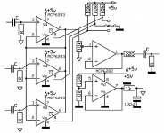
Updated the 4066 based circuit with inverting configurations for both op amps, the THD results at 1M and 1K input biases. I tried to keep all resistors under 50K, it affects the impedance after the 4066 and creates a HPF with the input coupling cap. It changes the BPF response as well. THD is much better than the non-inverting configuration and JEFT input switch. I still couldn't get logical looking noise spectrum graphs, values around 50 V/sqrt(Hz)??
1M
Source: 9.83e-7%
2.13e-7%
2.13e-7%
6.46e-5%
1.82e-7%
4.14e-6%
4.14e-6%
3.42e-6%
3.41e-6%
Output: 3.42e-6%
1K
Source: 3.15e-6%
3.89e-5%
3.89e-5%
3.93e-5%
3.89e-5%
4.05e-5%
4.05e-5%
3.91e-5%
3.90e-5%
Output: 3.91e-5%
Attachments
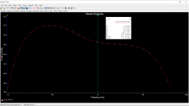
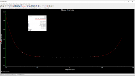
The graph in dB looks like input referred noise. This measurement makes it easier to compare noise performance of different circuits. It is the output noise divided by the gain of the circuit In this case gain is almost 1.
E.g. an opamp with input voltage noise spec of 5nV and gain of 12dB will have 5 x 4= 20nV output noise.
FET opamps have rising noise at low frequencies and sometimes at high frequencies. This gives the U shaped curve. Datasheets give noise plots for voltage noise and current noise. Current noise is the result of interaction of the opamp input stage and input impedance. In the case of FET opamps current noise can be ignored if input impedance is not too high. The other main source of noise is current noise in the input resistors. All components sum to give the final noise profile.
The other curve has no reference for what is being plotted. Graph says V or A. Which is it?
Last edited:
Thank you. I feel the lower and upper frequencies are related to the BPF. The graphs are V/sqrt(Hz) or A/sqrt(Hz), I'm not sure why it's not just V/sqrt(Hz).
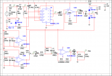
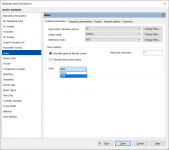
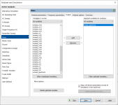
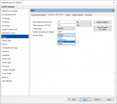
For the same circuit, here is the noise analysis setup tabs I'm not certain how to set it up properly.
For the same circuit, here is the noise analysis setup tabs I'm not certain how to set it up properly.
Attachments
As I am not familiar with your simulator I can only interpret.
A reference signal source and node has to be selected which in the majority of cases will be the signal source with theoretical zero noise. The node will also be the signal source node. This is the first setup panel.
Some simulators offer options for input referred noise which means you not have to calculate it. Others only give total noise. You can make a test circuit to determine or refer to simulator documentation. In this case since gain is almost 1, spectral input referred noise and output noise will be similar. Options are noise either as a frequency dependent plot or as total noise as you would measure with a meter which sums the noise over the setup bandwidth.
Pick a node(s) in the circuit for the measurement. This is the second setup panel. In a complex circuit this will help determine where in the circuit, the biggest noise contributions occur.
The last panel is for measurement bandwidth, accuracy and display format which has reasonable vales as shown.
- Status
- This old topic is closed. If you want to reopen this topic, contact a moderator using the "Report Post" button.
- Home
- Source & Line
- Analog Line Level
- Yet another mux, 4052, 4053 or 4066?