The DC voltage is as designed at every test point listed above in both 1M and 1K tests. I'm using the TL072 model for the buffer and output op amps and an LM358 for the voltage references.
I may use this configuration in the real circuit implementation, TL072s for the audio and LM358 for reference voltages. If the LM358s are the problem then I can swap them for something cleaner but I thought they shouldn't be much of a problem.
I may use this configuration in the real circuit implementation, TL072s for the audio and LM358 for reference voltages. If the LM358s are the problem then I can swap them for something cleaner but I thought they shouldn't be much of a problem.
Take a look at the High voltage MAX14xxx series.... , max +-36V, low Ron and extremely flat, 0.03 ohm at +-20V supply.... The MAX14756 Spec is 0.001% THD+N at 1K load.... They have a number of parts with different configurations. Only downside I see is the high off capacitance.
Removing C3 and it's resistor brought the distortion down to 0.0384% with 1M and still less with 1K at 0.00159862% with some points in the middle having higher THD still.
Changed the reference voltage op amps with TL072s, 0.0384% and 0.0017771%.
Changed them for DC power sources, 0.0384% and 0.0018%
So that's ruled out.
I'm still yet to test each section alone.
Edit: after disconnecting power to reference voltage circuits to isolate them totally, 0.0022% at 1K, leaving me more confused.
The TL072 model manufacturer is Texas Instruments themselves so I can trust them, 4066's is IIT which I don't know. There are models for 74HC4066 which is an analog switch as well but a different variant, what do you think?
Last edited:
Well, in the fourier settings, there is the amount of time it lets the circuit run for before sampling, it was set to 0.0001 seconds, I set it to 1 seconds which is an overkill, I also set the transient analysis options to start the analysis with the sim calculated DC operating point as the initial circuit conditions. This is very realistic as it lets whatever capacitance needs to charge to the DC operating point take it's time.
In the previous reply when I said I checked the DC operating point, I checked it in the interactive analysis not the DC component of the fourier analysis which is wrong! I'm not sure if the transient analysis initial circuit condition setting was previously set to "Determine Automatically" or "Set to zero" but when I ran it again at the 0.0001 seconds and zero inital conditions, the DC components in the FFT were not the correct values as I expected.
The input signal has a THD of 2.006e-6% for reference.
RESULTS:
at 1K bias and same 15K load: 7.36251e-5 %
at 1M bias: 0.000126456%
It's still unclear to me why the 1M has more THD.
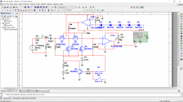
The full circuit, with a 1 ohm resistor for the 12V power source,
15K load, 1Khz, 15 harmonics, LM358 voltage references, TSTOP 10 seconds
Source THD: 3.55508e-10%
1M: 0.000126453%
Source THD: 4.65486e-6%
1K: 0.000110409%
Note: THD increases throughout the different stages as one would normally expect
15K load, 1Khz, 15 harmonics, LM358 voltage references, TSTOP 10 seconds
Source THD: 3.55508e-10%
1M: 0.000126453%
Source THD: 4.65486e-6%
1K: 0.000110409%
Note: THD increases throughout the different stages as one would normally expect
Last edited:
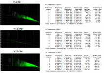
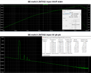
Here is a test in LTspice to illustrate the configurations match expectations.
The sim start time is 4mS. End time 12mS. Timestep 200nS.
The inverter method is compared to the buffer method at 1M ohm and 1K ohm impedance.
The test is setup to exaggerate switch distortion with a SS model that has higher resistance.
One thing that showed up was the type of opamp determines output swing in the buffer version. The inverter method does not have this sensitivity because the input swing is low. The larger input swing of the buffer can cause some inputs to bottom out early at this supply V. The TL072 seemed ok when I ran a check in TINA.
Although the inverter looks a lot worse, in reality with a lower switch resistance, the lower opamp distortion might mean it fares better than the buffer. A noise test shows the buffer is better on this front.
Attachments
Last edited:
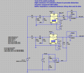
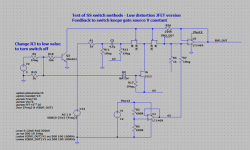
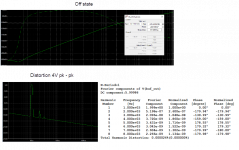
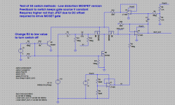
It is worthwhile including a technique that cannot be used with integrated solutions. Here is a discrete FET switch with very low distortion due to feedback from the buffer to maintain a constant gate - source voltage. The inverter method obviously cannot implement this without another inverter.
In a single supply situation it is fairly easy to make the switch logic compatible as shown in the sim file.
It may seem to have a bigger footprint than a 4066 type switch. If a complete switch is used to improve off state using multiple switch sections, then the FET solution looks more attractive. Dual FET SMD packages eg. CPH6904 from On Semi reduce the footprint further. This is a 25V 125 ohm device so can handle a decent swing.
The J113 used for sim should perform like the CPH6904. The off state is -105dB at 20Khz. This will improve when the buffer is driven by another input at lower impedance than 1Meg buffer bias.
Attachments
spladski - that's a neat solution. Makes you wonder whether some ICs might not be doing something like this...
Another little trick worth mentioning when dealing with CMOS switches having variable r_ON over the Vss...Vdd range that isn't centered around midpoint: Pick slightly asymmetrical (split) supply voltages so that a "real ground" reference (quieter!) lands the signal in the ideal zone.
Also, consider applying input bootstrapping if you need a real high impedance buffer input >1 Megohm.
I wouldn't have thought of running the switch into a virtual ground node. Chapeau, Mr. Self!
Last edited:
The SSM24xx series of switches jean-paul listed used this method, and included ramp generation for clickless action, but the parts went obsolete which is a shame. If they had stuck to DG style pin out they may have been more successful. I am not aware of replacements. If anyone does, let us know.
I'm not sure I really quite understand the difference now. I don't understand why the inverter has lower input swing. From what I saw in the datasheet, I think I'm confident that the TL072 will not clip at these input levels of 3.472 Vp2p. Since I'm confident about the swing, I think optimizing for the noise would be the way to go so the buffer it is I guess.
I'm still writing code for the digipot but I put the rest of the circuit together on a breadboard with battery power. I listened on monitor headphones, left channel was the circuit output and right side was the input to compare. I (23) couldn't discern a difference, someone else said the right side (input) was ever so slightly clearer. Remember, breadboard, trimmer instead of digipot and a feedback resistor nominal value in the final amplifier was 3.63K instead of 3.6K which may change the BPF slightly. It's picking up interference that goes away when I touch the circuit ground, I don't think that is op amp instability. I only have an analog scope so no FFT, I may use the PC sound card still.
I'm looking to reduce the switching "click", I can "mute" the digipot while switching inputs but I haven't tried that out yet, the click may still come through. I can try to PWM the 4066 switch inputs to ramp up and down, with an inaudiable frequency of course or maybe a LPF for that PWM and input an analog-ish voltage to the switch inputs?
I got lost pretty fast in TINA.
Your FET implementation is very attractive to say the least. Pairing the CPH6904 with a dual opamp SMD part would be ideal I guess. I just do not really get the schottky placement really, are you using the its small reverse leakage current to turn on J6? If I'd order parts, I'd try that out, but meanwhile I'm stuck with 2N7000 FETs which I'm not sure how audio worthy are they.
I was looking into reducing bias resistor values in the current 4066 based schematic, we got the 4066 biasing part settled at 1M but I'm thinking the digipot section might benefit from a higher input biasing current? I'm not sure what can be the consequences.
Last edited:
In the inverter example the input and feedback resistors form a potential divider at the inverting input of the opamp. Therefore, if the input signal is +1, the output signal is -1, the inverter input sits at almost zero. That is why it is referred to as a virtual ground. Inverter opamps do not experience much swing at the input. The buffer sees the full swing of the input voltage. I would suggest background reading for more info. Opamps not designed for low voltage can have inputs clip early. LT1057 seemed to have this issue. TL072 seemed ok.
The Schottky diode is to block positive V when the logic switch is closed, 1V and above. J6 has to have the opposite control to the switch JFET. On for JFET is when gate-soutce is 0V or higher. The gate needs to be more neagtive than on voltage relative to the source for JFET switch-off. In this case ground is negative as the reference is 6V. The voltage drop of the Schottky allows the gate to be pulled within 0.3V of ground to keep the JFET off at max input signal. Low gate-source on voltage JFET is needed to get the max signal swing.
bucks bunny showed a solution with 2N7002 without the center tie for improved off state. The JFET switch can be adapted to work with 2N7000 but this is enhancement device, positive gate for on and 0 - negative for off. Another opamp would be needed to drive the gates at a DC offset above reference voltage for the on state.
Sound quality will be limited by opamp and Digipot. The opamp bias resistor can be increased for lower switch distortion. Higher impedance needs good board layout. There is no benefit I can see to lowering impedance that the Digipot sees. The TL072 is long-in-the-tooth and has limited drive. Modern equivalent OPA1652 has wider low V swing and is substantially better in all parameters except slew rate and not expensive.
Last edited:
Okay so the problem is about the input swing not the output, I'm not sure I can find that in the datasheet like maximum differential voltage or something.
I may try the 2N7000, but it will be bulky. If it really makes a discernable difference I may consider about 10 of them in the final design.
Okay, I never studied depletion mode FETs so that's why I didn't get the circuit at first. I have what I think might be more modern op amps, MC33078, but it's a BJT not JFET input.
The 2N7000 has a gate source voltage spec of 3V. The gate drive needs to be more than 3V above the reference. The higher the better. This then has the prospect of the gate drive opamp clipping due to 12V limit. Check that first.
These devices also have much higher capacitance than JFET. Since the buffers are high impedance the non linearity of the MOSFET capacitance may be causing issues and better suited to low impedance situations. Try lower value bias resistors.
These devices also have much higher capacitance than JFET. Since the buffers are high impedance the non linearity of the MOSFET capacitance may be causing issues and better suited to low impedance situations. Try lower value bias resistors.
Here is the modified buffer feedback version with MOSFET 2N7002. These have 2.5V gate switch-on. The rail had to be raised to 15V. Distortion at least in sim seems ok.
I realized after posting this, that the gate drive opamp can also be fed from the switch output.
I realized after posting this, that the gate drive opamp can also be fed from the switch output.
Attachments
Last edited:
- Status
- This old topic is closed. If you want to reopen this topic, contact a moderator using the "Report Post" button.
- Home
- Source & Line
- Analog Line Level
- Yet another mux, 4052, 4053 or 4066?