The 5K load is just an approximation of the minimum impedance following the switch. There's a potentiometer, a band-pass filter with a gain of 0.5 and an op amp.
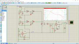
I had this pre-liminary schematic, the switches are set to have an on resistance of 132 assuming 4066 with VDD = 12V and an off resistance of 100M, the 10K pot is a digi-pot MCP4131-103E/P. I plan to use NE5534s instead of the LM358 as they're jsut for the simulation. I have a few LF351s that may come in handy too.
Suggestions for the schematic are more than welcome!
I'm not able to order any better switches right now, my best bets right now is to go with the 4066, I did a quick hearing test and it seemed quite good, haven't been criticial yet, studio monitors still holstered.
@00940 I've found a varient of that and already have it in my schematic and tested it, I'll test the one you referenced too but I'd prefer not using 8 opamps, 2 amps x 4 inputs. I don't like using dual or quad op amps for various reasons, cross talk distortion and reduced performance due to the increased dissipated power in the package. I know cross talk is fairly low but I already have some noticable in the amplifier that this circuit will be attached to, which I'm stuck with for the moment.
Regarding the schematic, the bottom LM358 is the 2.5V reference generator, in the real circuit I'll use a better op amp or a linear voltage regulator, not sure which is better atm.
Last edited by a moderator:

")
The Self scheme is inverting, also has a noise penalty with the input resistor. LF351 could perform the role of the high impedance buffer at the junction of the switches, its output connected to the pot. If the opamp runs on 12V, diode protection for the digipots at 5V would be needed.
The output swing of the LF351 does not reach the rails. In the attached buffer example, the ref here is raised to 3.5V and a cap to AC couple. You may need to raise it higher. The pot ref is 2.5V.
U3A will amplify the reference voltage by R9/R16. I don't think that is intended?
The output swing of the LF351 does not reach the rails. In the attached buffer example, the ref here is raised to 3.5V and a cap to AC couple. You may need to raise it higher. The pot ref is 2.5V.
U3A will amplify the reference voltage by R9/R16. I don't think that is intended?
Attachments
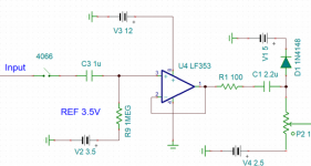
The scheme I used improves on Self's as it replaces the input resistor with another 4066 switch so there goes the noise penality at this point.
What I'm saying is what if I go with the configuration in my schematic, meaning that the buffer or rather here an amplifier is after the pot not before it. Also what if I use a buffer just after all the switches are collected to a point and before the digipot?
The signal should be 1.736 V peak or 3.472 Vp2p so if everything is playing nice it should be well within the 5V of the digipot but protection is necessary of course.
U3 has a filter before it with a gain of 0.1 not 0.5 I'm sorry made a mistake there. The amplifier has a gain of R9/R16 to try to raise the output to the same level as the input, I remember I attenuated the input with the filter gain at 0.1 not to clip, these values are just preliminary. At the time I was just trying to make it fit to work with a 5V supply but seems that can't be the case, not without a boost converter at least. In hindsight I really don't know why I decided to attenuate then amplify, seems pretty pointless now, wonder why it didn't at the time.
If you don't mind the signal inversion then the resistor can be replaced. But also the feedback resistor must be changed to a value matching the resistance of the switch otherwise there is gain. The distortion is generated because the switch resistance change is a big percentage of the resistances connected to it. Therefore, you will lose the distortion reduction.
The scheme I showed has only one switch in the diagram. You can assume that all selector switches join at the input capacitor. One buffer for x number of input selection. In this case the switch resistance change is compared with 1M ohm input impedance. Since this is a very small percentage, the distortion will be low. I.e. if the resistor change is 50 ohm, then (50/1000000)x100=0.005% as a rough indicator of distortion.
The scheme I showed has only one switch in the diagram. You can assume that all selector switches join at the input capacitor. One buffer for x number of input selection. In this case the switch resistance change is compared with 1M ohm input impedance. Since this is a very small percentage, the distortion will be low. I.e. if the resistor change is 50 ohm, then (50/1000000)x100=0.005% as a rough indicator of distortion.
Last edited:
Oh that's clearer I understand now. In my schematic I had the input AC coupled and shifted before the 4066 switch so that it's within the input range or do you assume in your schematic that it's still present?
In my schematic I referenced everything to one 2.5 V line to minimize the number of sources of distortion but I just can't wrap my head around how I can edit that into your schematic.
I think the 20-20k RC bandpass filter won't be a challenge, I'll adjust that by the end.
I also have some NE5534s, TL072s and MC33078s, I'm not sure which combination to use, would love suggestions on that too.
...brig001 I'm not sure what do you mean by a mixer, can you please explain?
I use a mixer like this Loop Mixer - 5 channel stereo audio mixer with loop function - Product/APP | Maker hart Industry Corp. but you could easily DIY one (it's on my list)
This way, there's no switching. All inputs are always on and you can 'select' by only playing the sources that you want to listen to. Doesn't suit everybody, but my wife is into karaoke and likes to sing along to TV, iPad etc. so this suits perfectly
Brian
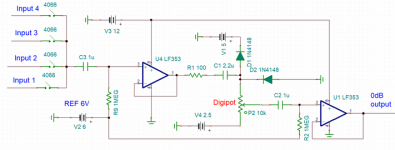
The buffer scheme is a template. Forum members are here to help improve your understanding, not complete the design. You must apply suggestions to your environment. The output sits at 6V so that will need AC coupling.
The voltage ref can be provided by a simple pot divider as shown in the attachment. However an opamp buffered pot divider can provide a stiffer reference. The LM334 can also be used.
The TL072 has 2 sections so it is the more compact solution and has lower noise and bias current than the LF351. The 5534 can be used if driving low impedance is required as the output buffer. The bias current will cause additional DC offset but this is not an issue for AC coupled output.
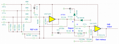
The attachment shows a generic solution for higher level inputs with other switches which need to be attenuated to feed the Digipot. There is 11.8dB attenuation and gain make up to bring the overall gain to unity.
The reference for the buffers is below half rail to match the flattest part of the switch resistance curve to give lowest distortion. If a 5534 is used as the output buffer the opamp input will be lowered by another 0.5V.
The voltage ref can be provided by a simple pot divider as shown in the attachment. However an opamp buffered pot divider can provide a stiffer reference. The LM334 can also be used.
The TL072 has 2 sections so it is the more compact solution and has lower noise and bias current than the LF351. The 5534 can be used if driving low impedance is required as the output buffer. The bias current will cause additional DC offset but this is not an issue for AC coupled output.
The attachment shows a generic solution for higher level inputs with other switches which need to be attenuated to feed the Digipot. There is 11.8dB attenuation and gain make up to bring the overall gain to unity.
The reference for the buffers is below half rail to match the flattest part of the switch resistance curve to give lowest distortion. If a 5534 is used as the output buffer the opamp input will be lowered by another 0.5V.
Attachments
A recent app. note from TI: https://www.ti.com/lit/an/slla471/s...tiplexers%2Fanalog%2Ftechnical-documents.html
@spladski I really appreciate everyone's help, I do not mean to ask anyone to design anything, I'm juts trying to understand different points of view in different aspects of the design.
In my original design I referenced the audio signal to a single 2.5 V line from the input all the way to the output not to have many sources of distortion; not to have to deal with noise on multiple refernce lines. In your design I see you add the offsets as a voltage divider from the power supply rails and feed it to all but the digipot which confuses me, any particular reason to separate them?
I'm not sure which part of the switch resistance curve you are talking about can you please clarify that.
What if I attenuate each channel before each switch? Regarding the system input impedance I assume 25K is about perfect but I'm not sure about the 4066's point of view. Having each input separately attenuated is because some devices connected to the inputs might be expecting a lower impedance load, still thinking it through, might not be a good idea afterall.
@mickeymoose thank you, will definitely give it a good read!
@mchambin they give the curves for the switch resistance in various conditions which I assume helps to estimate THD for a given circuit but that's a part I haven't got a chance to study yet so I'm here learning my way through.
The scheme is split into 3 sections: When you AC couple, you must provide a reference for the signal swing. In a +/- V supply system, this is ground. In a single supply system it must be half or approx, of the rail. The signal will swing above and below the DC voltage on the output side of the AC coupling cap.
1. Input switch and buffer section. This runs on 0 - 12V. So its center point is 6V.
2. The Digipot. This runs on 0 - 5V. So its center point is 2.5V. Since the signal swings above and below 2.5V we must place the base of the pot at 2.5V. If we ground the base of the pot, terminal B, then the signal will attempt to swing below ground. We can't have this because the signal must remain within the PSU of the Digipot.
3. Output buffer section. This runs on 0 - 12V. So its center point is 6V.
All sections are AC coupled to allow different DC references. Since the input and output sections have the same supply, they can use the same reference.
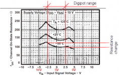
The attachment shows how you must adjust the scale of the curve according the supply situation, in this case 0 - 10V because the curve is plotted for 10V or +/- 5V. You can see that sliding the window for the Digipot swing can result in a lower resistance change. So we apply an offset to the center point for least resistance change.
1. Input switch and buffer section. This runs on 0 - 12V. So its center point is 6V.
2. The Digipot. This runs on 0 - 5V. So its center point is 2.5V. Since the signal swings above and below 2.5V we must place the base of the pot at 2.5V. If we ground the base of the pot, terminal B, then the signal will attempt to swing below ground. We can't have this because the signal must remain within the PSU of the Digipot.
3. Output buffer section. This runs on 0 - 12V. So its center point is 6V.
All sections are AC coupled to allow different DC references. Since the input and output sections have the same supply, they can use the same reference.
The attachment shows how you must adjust the scale of the curve according the supply situation, in this case 0 - 10V because the curve is plotted for 10V or +/- 5V. You can see that sliding the window for the Digipot swing can result in a lower resistance change. So we apply an offset to the center point for least resistance change.
Attachments
You must evaluate the clipping behavior of each circuit section to determine if attenuation is needed. This is going to be limited by the opamps since their swing does not reach the rails. Datasheet for this information, which usually gives output swing for load and supply V.
The input impedance is the bias resistor for the opamp buffer 1M. If you need a specific load impedance then this should be applied before the AC coupling cap at the input. In most cases it wont be needed.
I would advise becoming familiar with LTspice or Tina free simulators. This is the fastest route for self tuition. Mooly on this forum provides guidance on the use of LTspice for beginners.
Installing and using LTspice IV (now including LTXVII). From beginner to advanced.
So if I understand correctly, for the 25 degree C curve I should probably use even lower than 4.9, possibly 4.0 V, am I correct?
So attenuation trimmers before the input cap is not a problem then.
I use NI's mulitsim which I'm most familiar with, I presume its spice models are fairly accurate. I also use Proteus for quickly putting stuff together. I also tried to use Tina but there where parts I couldn't find so I just stuck with Multisim.
- Status
- This old topic is closed. If you want to reopen this topic, contact a moderator using the "Report Post" button.
- Home
- Source & Line
- Analog Line Level
- Yet another mux, 4052, 4053 or 4066?