I actually needed an excellent buffer for a different project. Your buffer was the only one that was helpful. So, I'm grateful for it.Hi Dan, tell me if you want a pair of Kuartlotron boards. I still feel a bit guilty about your disappointment with the Kuartlotron, with it not being a bass enhancer and all... But I swear, that one time it really did!
It did not change the tone or resolution (I said that earlier in a funny way).
Also, it doesn't put gain on its power, so providing adequate power was much easier and lower cost too.
Not having to finesse the power as much as an amplifier or preamp would need, was a really wonderful convenience, that I hadn't seen before.
I'm not disappointed in the buffer, and I don't need boards because I can build them coin size almost as fast as I could solder boards.
P.S.
However, I'm ever so curious about that lost, early, prototype. It had a surprisingly tiny parts count for the job it was doing.
Well, I'm having some trouble trying to solder the miniature 'donuts' on the underneath - you could double the size and also double the clearance between these and the ground plane and mask
Increase the space for resistors up to about 10mm so can fit 0.4W and 0.6W units
Change the tracks to the bottom layer and the ground plane to the top layer - maybe also add 0volt tracks for the power caps, separate to Gnd plane and signal gnd
Increase the allowed space for the capacitors - up to 16mm for the Nichi BPs, BGs, etc - at present limited choice by small space
Move the input/output connections closer to edge &/or separate signal and power terminals - also, move test point TP to outer edge and R11?
Allow room for 12mm PP, styrene, etc cap (C3 - 15pF)
Perhaps 2 designs, one for large resistors/caps/board and another for small smd version?
We all have different ways of doing pcbs so above the suggestions are just suggestions
All the best ...
You don't want pins going through a ground plane for EMC reasons, otherwise I may have made the top the ground plane.
The I/Os are meant to be compatible with terminal blocks, since some people insisted on it. It certainly helps with experimenting. Maybe I should reclaim some space by making the blocks bottom mount? That would help with many of your suggestions, which require more space.
Signal ground, capacitor return and ground plane are separate already, although it may not be obvious.
Ah, I didn't now there was EMC problems with holes in a ground plane - doesn't apply to the component holes? Ideally, smd components only on the one layer?
Can bigger clearance holes, irregular shaped apertures, slotted/sectional planes (as per Tentlabs), etc reduce the EMC reasons or does any/all perforations create problems? [Is it a design protocol and how significant to sound quality would it be to ignore it?]
Maybe a bigger size would be a reasonable compromise - it is a very tidy, neat little board
Perhaps you could include spacing for some right angled terminal blocks for top/bottom mounting too - not sure if you can easily get them with 7 pins but maybe 4 & 3?
Ah, signal ground (SG) 'via' to ground plane (and PG) for R7 and C3.
I asked about the size of resistors because 1/4w was a little tight, but I think .4/.6w is a bit excessive. Is it easy to get different 15pf caps that size? I looked and it was mica or ceramic with Mouser. I prefer film that smooths out signal in the case of being a bypass for over the audio band.
Although I have to say a second PG via wouldn't hurt, I just soldered mine together on the bottom.
Wouldn't price go up if they aren't printed on the DirtyPCB 5x5?
Although I have to say a second PG via wouldn't hurt, I just soldered mine together on the bottom.
Wouldn't price go up if they aren't printed on the DirtyPCB 5x5?
I'll 2nd the size of the pads on the bottom. I haven't started soldering yet, but I think they'll be a small bit of a challenge.
I'm not one to usually go cap rolling or resistor rolling on boards, so I have no complaints as I'll go with what you specified for the board.
Only other thing that I can think of is that I'm not used to seeing such a thin board but I suppose this was a performance consideration that guided you to make the board with that thickness. All in all, I'm happy with what I got.")
I'm not one to usually go cap rolling or resistor rolling on boards, so I have no complaints as I'll go with what you specified for the board.
Only other thing that I can think of is that I'm not used to seeing such a thin board but I suppose this was a performance consideration that guided you to make the board with that thickness. All in all, I'm happy with what I got.
You don't want any pins passing through a ground plane such that the ground plane forms a turn around the pin, because then you get a lot of unnecessary current induced in the ground plane which can couple to all the other pins passing through it. The solution is to make a slot in the plane between the pin and it's return current, but if I did this with the entire board the ground plane would be cut into tiny pieces and completely neutered. I intended the ground plane to have minimal interruptions, and this is one reason for the small pads on the bottom, so they don't cut the ground plane apart.
The boards are thin because it makes the ground plane work better.
12mm is enormous for a 15pF cap. If you think about it, your input cables will have 10 times or more capacitance. I was planning to to increase the pad size to 7mm, to accept common silver mica caps.
The boards are thin because it makes the ground plane work better.
12mm is enormous for a 15pF cap. If you think about it, your input cables will have 10 times or more capacitance. I was planning to to increase the pad size to 7mm, to accept common silver mica caps.
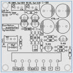
Here is the new PCB I'm thinking about. This is more how I originally wanted to layout the PCB but couldn't make work. It's also more compact, which means I have just enough space to add some TL431 shunt regulators, which seems to be a good idea since so many people were asking about the PSU.
I don't know if I can do that and also add 10mm resistor pads. I would suggest for people to just add the resistors standing up if they want to use bigger resistors. Most of the resistors aren't in the signal path and will hardly affect performance at all.
The transistors are a bit further apart so for thermal coupling the leads will be bent slightly or they can be coupled with a small metal plate.
Attachments
Yes, when they're too big for a fast thing, that's when you need to bother adding the coil; however, if they were small enough, then a resistor will do fine for series element. So, the best complaint I have managed is an awfully unimportant nitpick.Does anyone have complaints about the PCBs? Eventually I may want to order more and can make some changes.
I'm just saying that when it is fast, make it smaller, much smaller. I do love the capability of this buffer to make the source signal a really tiny bit better, BEFORE magnifying that forty times with my amplifier. Even though not all of my applications have the need, I'm still sure it is worth doing for cases when we wanted high quality. So much, that now when I do something without it, then I'm wondering if it shouldn't be doing just a bit better if I added four more transistors . . . before applying gain. Lesson learned. Meanwhile, back to the topic. . .
I was informed it was supposed to be a fast thing and therefore I built it as small as I could, coin size, before reviewing it; because, I wanted to hear and review Kean's design, not my error.
A cost is that I'm ignorant of what it sounds like with a large size sprawling layout. A large layout is not relevant for a fast thing; and, therefore, I recommend that a layout be very small in size.
The 0000 or 000 steel wool lasts until I lose them all. I lost a whole package of that. Probably it would have lasted indefinitely to clean off the soldering iron.I only have problems with it when my soldering iron is dirty. Put some solder on it to break the layer of crust, or wipe it off with a paper towel or cloth.
Also, Gel Flux, recently discontinued because Radio Shack went out of business, is a combination of Rosin flux with petroleum jelly, and that really did help in making the soldering elementary, working perfectly on the first try. Even though it was sticky, it was ever so shiny, and that's how you knew the connections were perfect. Sure, the cleanup was a bother (Simple Green + Alcohol/GermX), but you could test out the circuit before cleanup, and there wasn't any trouble with bad connections. So, where do we buy the Gel Flux now? And, how on earth do I do all that point to point stuff without it?
The solder isn't what you were after--it is rosin core solder and what was needed was the flux. Where is the goodly flux now/today?
I suppose I wouldn't mind some cleaning, if it had very good results. Plenty of good leads here:
https://www.ixquick.com/do/search?q...elly+rosin&cat=web&pl=chrome&language=english
What makes the need for the coil is the transistor junctions being slow, not the wiring. Even with a very compact layout the inductor would be beneficial. The ground plane helps with a lot of the concerns of a finitely small layout.
Last edited:
Here is the new PCB I'm thinking about. This is more how I originally wanted to layout the PCB but couldn't make work. It's also more compact, which means I have just enough space to add some TL431 shunt regulators, which seems to be a good idea since so many people were asking about the PSU.
I don't know if I can do that and also add 10mm resistor pads. I would suggest for people to just add the resistors standing up if they want to use bigger resistors. Most of the resistors aren't in the signal path and will hardly affect performance at all.
The transistors are a bit further apart so for thermal coupling the leads will be bent slightly or they can be coupled with a small metal plate.
Make it a stereo board with PSU and inputs and outputs of both channels grouped together at opposite sides of the PCB (like in real life when it is built in a case). Inputs at the side where volume control is, outputs at the back of the board where the outputs normally are situated. Power supply pads at the side where the PSU is to be located. Add some pads for a volume control at the side that is looking at the front of the case to make mounting a volume control (of any kind) a breeze. Best things in life (like some extra solder pads) are free
That is how 99% of builders will encase a board, no one likes to cross input and output wiring and it is better not to do so technically. Connectors in the vicinity of where the RCA connectors are make for tidy wiring and easier fault finding when something does not work too. Shortest possible signal path etc etc. All common stuff and common rules created by necessity. Why make it more difficult for builders, technically less optimal and less esthetically pleasing ?Why mono boards in this day and age ? Stereo boards save from drilling excessive mounting holes too and it makes for less wiring (and also tidier and easier wiring). I can not see the reason sticking with module like mono PCB's as I think there aren't any positive features involved. I think true mono users will be less than 0.1% of builders. Multichannel people also will like stereo boards than can be stacked. I got the very nice looking boards from nattawa a long time ago but haven't found the time to populate them completely. They look quit intimidating with so many SMD parts but I will succeed one day.
Last edited:
Since the buffer is and should be universally usable I think that single channel boards are useful. Not everything nowadays is "stereo". I like the "mono" concept a lot.
The buffer board could be made even smaller, something like a plugin board with 2.5RM plugs or sockets. Then everybody can design their own "motherboard", in stereo or multichannel, which also supplies the voltages, inputs, outputs etc. Using smd parts it could be even half the size it is now. Thus said, I like the board also as it is, inspite the little fault.
The buffer board could be made even smaller, something like a plugin board with 2.5RM plugs or sockets. Then everybody can design their own "motherboard", in stereo or multichannel, which also supplies the voltages, inputs, outputs etc. Using smd parts it could be even half the size it is now. Thus said, I like the board also as it is, inspite the little fault.
- Home
- Source & Line
- Analog Line Level
- The Kuartlotron - keantoken's simple error-correction superbuffer