Hi,
just some ideas about discrete Buffers for Line-Level.
I was a bit surprised that I couldn´t find some of these Buffers here at DIYaudio, so I thought I´d give it a try.
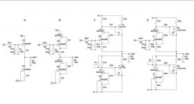
Starting with ´A´ the well known and very simple CCS-loaded Source-follower. This can give already good distortion figures and a Buffer can´t be much simpler than that. If J1a and J1b are matched -matched Duals here- one can omit with output coupling caps if the input signal is free of DC.
Beeing a singleended circuit the maximum current into the load could only be once the bias current. This means that it can only drive highimpedance/lowcurrent loads well and heat losses in the JFETs are high.
With smallsignal high-gm JFETs also the supply voltages are usually restricted to less than +-15V.
´B´ is a cascoded variant of ´A´. Here J2a and J2b run much cooler, since the cascode JFETs J3 and J4 provide for low and nearly constant Drain-Source voltages. J3 and J4 may be high Idss low-gm types, which take over most of the heat losses. While the load drive capability is nearly the same as with circuit ´A´, the distortion figures are considerably lower. If J2a and J2b are closely matched, the output offset will remain low enough that no output cap is required, even with unmatched cascode JFETs.
Circuits ´C´ and ´D´ are an idea -I haven´t seen it here before, but very probabely it´s nothing new at all- to increase load drive capability.
It resembles characteristics of a Sziklay- or Compound pair and cascodes.
Circuit ´C´ could probabely named HCC, Hybrid-Cascode-Compound, circuit ´D´ could be called FCC, FET-Cascode-Compound.
Both only differ structurally by the useage of PNP resp. PMOS as output devices.
The voltage drop over the cascodes drain resistors are used to bias and modulate the output transistors.
The two circuits allow to drive much lower impedance loads than ´A´ and ´B´, due to the much increased bias currents (10x and more).
The extreme short and direct feedback loop of the Sziklay pair preserves the good THD-values of the cascoded JFET stage. Since the JFETs may run on smaller bias currents (more degenerated with larger source resistor values) and drain voltages, they run alot cooler. Temperature and temperature drift issues are lower. The Potis in the CCS-JFETs drain allows to tune the output offset, so that no coupling cap should be required. Tolerances of the PMOS might be checked though.
Headroom is lower than with the simpler circuits ´A´ and ´B´, especially with the PMOS output devices of ´D´. With +-15V supplies ´D´ is capable of 4Vrms which is more than sufficient for typical high-level applications.
´D´ shows slightly better THD than ´C´ with highimpedance loads, while ´C´is slightly better with lowimpedance loads and can drive up to 6Vrms.
Using the simmed devices (all in SMD) one could use the same layout for ´C´ and ´D´ for easy evaluation and comparison.
Does anybody recognize some hidden drawbacks apart from possible need of matching the PMOS?
jauu
Calvin
just some ideas about discrete Buffers for Line-Level.
I was a bit surprised that I couldn´t find some of these Buffers here at DIYaudio, so I thought I´d give it a try.
Starting with ´A´ the well known and very simple CCS-loaded Source-follower. This can give already good distortion figures and a Buffer can´t be much simpler than that. If J1a and J1b are matched -matched Duals here- one can omit with output coupling caps if the input signal is free of DC.
Beeing a singleended circuit the maximum current into the load could only be once the bias current. This means that it can only drive highimpedance/lowcurrent loads well and heat losses in the JFETs are high.
With smallsignal high-gm JFETs also the supply voltages are usually restricted to less than +-15V.
´B´ is a cascoded variant of ´A´. Here J2a and J2b run much cooler, since the cascode JFETs J3 and J4 provide for low and nearly constant Drain-Source voltages. J3 and J4 may be high Idss low-gm types, which take over most of the heat losses. While the load drive capability is nearly the same as with circuit ´A´, the distortion figures are considerably lower. If J2a and J2b are closely matched, the output offset will remain low enough that no output cap is required, even with unmatched cascode JFETs.
Circuits ´C´ and ´D´ are an idea -I haven´t seen it here before, but very probabely it´s nothing new at all- to increase load drive capability.
It resembles characteristics of a Sziklay- or Compound pair and cascodes.
Circuit ´C´ could probabely named HCC, Hybrid-Cascode-Compound, circuit ´D´ could be called FCC, FET-Cascode-Compound.
Both only differ structurally by the useage of PNP resp. PMOS as output devices.
The voltage drop over the cascodes drain resistors are used to bias and modulate the output transistors.
The two circuits allow to drive much lower impedance loads than ´A´ and ´B´, due to the much increased bias currents (10x and more).
The extreme short and direct feedback loop of the Sziklay pair preserves the good THD-values of the cascoded JFET stage. Since the JFETs may run on smaller bias currents (more degenerated with larger source resistor values) and drain voltages, they run alot cooler. Temperature and temperature drift issues are lower. The Potis in the CCS-JFETs drain allows to tune the output offset, so that no coupling cap should be required. Tolerances of the PMOS might be checked though.
Headroom is lower than with the simpler circuits ´A´ and ´B´, especially with the PMOS output devices of ´D´. With +-15V supplies ´D´ is capable of 4Vrms which is more than sufficient for typical high-level applications.
´D´ shows slightly better THD than ´C´ with highimpedance loads, while ´C´is slightly better with lowimpedance loads and can drive up to 6Vrms.
Using the simmed devices (all in SMD) one could use the same layout for ´C´ and ´D´ for easy evaluation and comparison.
Does anybody recognize some hidden drawbacks apart from possible need of matching the PMOS?
jauu
Calvin
Attachments
Also see this thread http://www.diyaudio.com/forums/solid-state/225255-jlh-buffer-homage-john-linsley-hood.html
Or you could search JLH buffer as there are a couple of older threads regarding it.
Interesting schemes. I think schemes C and D perform better if you use p channel fets, comparison would be interesting.
Or you could search JLH buffer as there are a couple of older threads regarding it.
Interesting schemes. I think schemes C and D perform better if you use p channel fets, comparison would be interesting.
Hi,
interesting hint. I´ll follow that.
The simulation results are so far very similar to the DADOD JLH-sim. Figures <-100dB. Noise sims are also extremly low ~0.3µVrms.
Basically I´d prefer a complementary lower part too (simply for double the output current), but there are no real complements and the stability over temperature and offset is very ok with the matched Dual NJFETs. The overalll parts number count is smaller and there´s a lower number of different parts. If matching is needed it´d be easier than with complementary devices. Trimming the SE- circuit should be easier with just one pot.
So there´s alot in pro of the SE-stage.
jauu
Calvin
I also wonder about the reproducibility of the bias currents of variants C and D when there is mismatch. You put some resistors in the second stage to reduce loop gain and thereby make the biasing more predictable, but maybe it would be better to do this:
reduce R19, R20, R29 and R30 to 0, less loss of local loop gain
connect the collector of Q1 to the top side of R11, and similarly the collector of Q2 to the top side of R12, drain M1 to top R23, drain M2 to top R24
The bias current of the JFETs is then set by VEB/R15 (VEB/R16) or VSG_M1/R27 (VSG_M2/R28), the VSG of the JFET and R12 or R24 sets the total bias current.
You could replace R15 and R27 with current sources to further reduce loop gain loss.
Calvin hi, I have a Cary CDP with this I think, in "A" given 15v rails, what do you estimate the output impedance to be before a series 100ohm output resistor that it has?
Thanks George
Thanks George
Hi,
with the Cordell model LSK389CCo following results simmed for Zout of circuit´A´.
R2/3: 1,0 mOhm -> Id: 8.64mA -> Zout: 34.7Ohms
R2/3: 4.7 Ohm -> Id: 7.63mA -> Zout: 41.1Ohms
R2/3: 10 Ohm -> Id: 6.78mA -> Zout: 48.2Ohms
R2/3: 22 Ohm -> Id: 5.47mA -> Zout: 63.8Ohms
jauu
Calvin
with the Cordell model LSK389CCo following results simmed for Zout of circuit´A´.
R2/3: 1,0 mOhm -> Id: 8.64mA -> Zout: 34.7Ohms
R2/3: 4.7 Ohm -> Id: 7.63mA -> Zout: 41.1Ohms
R2/3: 10 Ohm -> Id: 6.78mA -> Zout: 48.2Ohms
R2/3: 22 Ohm -> Id: 5.47mA -> Zout: 63.8Ohms
jauu
Calvin
Hi,
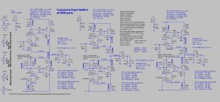
here are the sims of the dimensioned circuit variations of circuit ´C´.
The first is the original circuit ´C´, the second the variant after Marcel´s suggestions, the third is a conglomerate of both.
Bias values and simmed data is included on the sheet.
Marcels variant indeed improves a bit on some parameters, such as THD, IMD and Bandwidth. Idle currents through the JFETs are reduced, the currents and power losses through the bipolar outputs are increased.
It would be nice to reduce parts matching requirements by the use of degeneration resistors. So I simmed Marcel´s variant with reintroduced Emitter resistors. To my surprise improved this the thing even more.
The THD- and IMD-values are slightly better on a academical niveau.
The idle current through the JFETs is ~30% higher, which may make a positive sonic difference, since JFETs like to run hot. Power losses are still low enough for these SMD-packages. The idle currents and power losses of the bipolar output transistors are reduced and close to the orignal ´C´-circuit. Also reduced are noise figures.
Seems like a complete win at the cost of just two additional resistors.
jauu
Calvin
ps. interstingly didn´t current sources instead of R15/27 improve the THD-figures as expected. Lowest THD was still simmed with the Emitter degenerated circuit.
Attachments
Last edited:
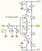
Hi Calvin, here is one that John Curl seemed to like and the DC offset trim works a treat. If you could sim it that would be nice. I'm using it and it sounds better than A in your first post which I had before.
Cheers George
Cheers George
Attachments
Last edited:
Hi Calvin, here is one that John Curl seemed to like and the DC offset trim works a treat. If you could sim it that would be nice. I'm using it and it sounds better than A in your first post which I had before.
Cheers George
Interesting. I wonder how it would compare to C and D.
EDIT: btw IMHO A sounds better than B
In what way does it sound better ?
Still referring to post 10? I would be curious to know that too 😎
In what way does it sound better ?
It seemed to have better more solid drive and dynamics into my Lightspeed Attenuator which is around 7k input, and the poweramp which is around 50k so it was seeing a total load of around 6k I don't know if this was the reason though.
Or maybe it's the fact that it can be dc coupled with the 250ohm trimpot which it is now trimed to .1mV offset, and steady once over the inital switch on bump of around .500mV but this quickly settles.
Cheers George
Last edited:
Hi Calvin, here is one that John Curl seemed to like and the DC offset trim works a treat. If you could sim it that would be nice. I'm using it and it sounds better than A in your first post which I had before.
Cheers George
You can improve this to bootstrap cascode.
Attachments
... here is one that John Curl seemed to like ...
I´m not aware of any John Curl schematic where this buffer was used.
(It´s from a chinese ebay seller if I´m not mistaken.)
What John did use, is a similar configuration without cascode for the
output of the JC-2 (ML-1) phono stage. It´s within the feedback loop
in this phono stage, though.
You can improve this to bootstrap cascode.
Arent the Jfets in the original post 10 already bootstrapped, the only diffrence is that you are removing the 22 ohm resistors.
- Home
- Source & Line
- Analog Line Level
- Preamp-Buffers - simple idea