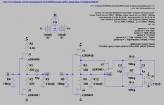
Here is an even easier, simple circuit that has only 2 jFET's and 3 resistors:
Using +22 and -22 vdc supplies, 2H and 3h and beyond are all <-120dB. R4 nulls the THD to almost nothing without cascoding.
Thx-RNMarsh

Using +22 and -22 vdc supplies, 2H and 3h and beyond are all <-120dB. R4 nulls the THD to almost nothing without cascoding.
Thx-RNMarsh
Hi,
I wouldn´t use fixed resistors from the start, but either of two options.
The optimum degree of current source modulation is load dependant.
The poti-setting differs between low-impedance/high load-current loads and high-impedance/low load-current loads and should be set after the lowest load impedance one expects and highest current swing symmetry.
The first option beeing to solder pots permanently.
Bürklin lists a decent range of 3mm², 4mm² SMD multiturn pots from Bourns and BI-Tec as does Digikey with several vendors up to Vishays MetalFoil.
The second using pots provisionally to evaluate the right values and replace them with fixed value resistors permanently.
jauu
Calvin
Here is an even easier, simple circuit that has only 2 jFET's and 3 resistors:
Using +22 and -22 vdc supplies, 2H and 3h and beyond are all <-120dB. R4 nulls the THD to almost nothing without cascoding.
Thx-RNMarsh
View attachment 360321
And now the ATL handed me a DC coupled version 🙂
Attachments
Hi Frans
I believe the idea was to use a Nfet and a Pfet to cope with non linearities... Now the ATL adds another single fet as part of the servo.... does it comply ?
I believe the idea was to use a Nfet and a Pfet to cope with non linearities... Now the ATL adds another single fet as part of the servo.... does it comply ?
The opamp as a buffer alone will have less distortion then this one, but....
does it sound as magical ?
does it sound as magical ?
The simulator gives the same results for both circuits, except for the output offset, that is nearly zero with the servo. The added fet just functions as a resistor.
Calvin,
thanks for sharing your thoughts. I'll simply integrate both to the board 😀 Should be easily possible to add some additional pads for fixed resistors without too much additional board space.
BTW (@all): would you prefer 1ch or 2ch boards?
regards, Daniel
thanks for sharing your thoughts. I'll simply integrate both to the board 😀 Should be easily possible to add some additional pads for fixed resistors without too much additional board space.
BTW (@all): would you prefer 1ch or 2ch boards?
regards, Daniel
Hi,
single channel, 4-layer double-sided, all SMD, with PCB-board connectors to a motherboard, 104µm copper silver coated, Teflon, black solder resist and white silkscreen with my avatar as logo would make me happy ;-)
jauu
Calvin
single channel, 4-layer double-sided, all SMD, with PCB-board connectors to a motherboard, 104µm copper silver coated, Teflon, black solder resist and white silkscreen with my avatar as logo would make me happy ;-)
jauu
Calvin
sounds good 😀 what about embedded self-powering PSU (energy harvesting), wifi remote control,...😱
sounds good 😀 what about embedded self-powering PSU (energy harvesting), wifi remote control,...😱
Go nuclear (mmm... Germany is scrapping al nuclear 😕) 🙂

Hi,
so far so small ;-)
I´d try to get the In-out connectors all to one side with a single row of connectors.
The thermal for the power transistors may be a bit small. You may increase thermal capacitance by using the second copper layer also by thermal vias.
I´d also try to get the 3 casings of CFP-Master transistors in close proximity and glue a single cooling fin covering all 3. The left CFP-bipolar could switch positions with the passive component to its right. The right hand side CFP-block may be turned 90° counterclock-wise. The LSK shoved upwards, switching positions with the Poti.
Besides getting the 3 active devices close together it´d give way to place the power caps in the middle, closer together, reducing trace length and loop size, hence decrease inductance.
Omit with the T-connection to the lytics/caps. Instead use dedicated to- and from traces (V-shape).
For easy accessability the Potis are usually better placed towards the outer rim of the PCB. To keep most of the signal traces on one copper plane (every via means parasitics) I´d use SMD Pots.
I´d also add small inductances in series ahead of the power caps (e.g 600R@100MHz)
The pic is a cutout from a first attempt for the Hybrid-Compound Buffer (JFET-cascode). Two buffers on a single PCB of 80x40mm. Roughly 1/3rd thermals, 1/3 circuit, 1/3rd power supply lytics.
jauu
Calvin
Attachments
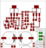
Look at the end clearance of resistors. You need enough room to insert your soldering tip.
A few resistors have very small end clearance, see the two, end to end, at the bottom and a couple up to the right of the central VR.
A few resistors have very small end clearance, see the two, end to end, at the bottom and a couple up to the right of the central VR.
Thanks guys,
i'll do some part shuffling this evening 😉
BTW: just realised that the pinout of the FZT751 in my layout program is wrong 😱 so i'll have to change that too. Not the first time that this happens with Target! 😡
i'll do some part shuffling this evening 😉
BTW: just realised that the pinout of the FZT751 in my layout program is wrong 😱 so i'll have to change that too. Not the first time that this happens with Target! 😡
Would it be possible to have the eagle files posted in a zip folder..??
I'll then work it over with the differential stage as well
I'll then work it over with the differential stage as well
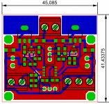
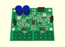
PCB for CFP2 v0.2
Hello all,
here's another version of a small board for CFP2. Overall board size is 48x40mm. Thermal pad area per power transistor is approximately 10x20mm each layer. Could be increased by increasing board size.
Pots are SMD now and placed more to the outer rim, active devices are close together and loop area of pwr supply has been reduced. In and out are on left and right side respectively, out could be moved to the left too if there is any problem with this config. PCB layout is always a compromise 😱
Again, any comments are welcome 🙂
MiiB: I am using Target! so posting files wouln't be of much help for you !?
regards, Daniel
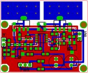
Attachments
Last edited:
- Home
- Source & Line
- Analog Line Level
- Preamp-Buffers - simple idea