I will publish the measurements later but here is what i found :
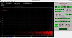
Frequency response of the Piglets Dad goes over 10MHz.
That is not new to me, the first Paradise buffer went there too and that could be a problem with oscillation. The PD is rather stable with a well damped overshot.
A simple RC filter at the input can tame that. PSSR rejection is very high, around -100dB.
Distortion at 1V is around -90dB, second, no third. Intermodulation showed nothing besides simple sidebands.
The Calvin is better in this regard. I could not measure anything with the Quant Asylum unless i really heavily loaded ( 80 Ohm in my experiment ) the output. So distortion is under -105dB, the resolution floor of the Quant Asylum.
The appearance of second in parallel symmetric design comes from matching differences of the PNP and NPN transistors. I expected that because i took the BC550C/BC560C right out of the stash without any selection. I assume a 10dB improvement could be made when the transistors are better selected. -100dB is absolutely the best that can be done in an open loop circuit. I know that from 5 years research on MPP. The Piglets Dad is open loop,
i do not consider a driven cascode as feedback. The Calvin has current feedback though so has a distortion reduction mechanism that goes beyond simple degeneration and matching.
Why did i build the Piglets Dad in the first place : it is a quick and very good fix when you do not have JFets. It is dirt cheep and can be build in less then two hours without any exotic components with what you have around.
By the way, DC offset was 5mV, again without any matching so this design is mature.
Last edited:
Hi,
@AndrewT
The bias current was chosen high. The CCS runs on ~37mA and each of the two branches thus on ~18.5mA. Of this the PNP takes on ~17mA, or ~95%, while the JFET runs on <1mA or ~5%.
The current distribution between JFET and PNP can be changed by varying the JFET´s Drains resistors R1 and R5. Decreasing the value raises the JFET´s bias and decreases the PNP´s bias. The THD (mostly K2, K3) slightly increases with K3 becoming the dominant harmonic.
The combined bias current was chosen so high because of twoandahalf reasons.
a- the required Source- and Drain resistors R2/3 and R6/7 could be kept small in value.
The source resistors directly affect on the noise figures. Lower values --> lower noise contribution.
b- a high ratio of bias current to signal current is usually good for low distortion figures. If You reduce the CCS-current to ~17mA (R13=39R) the THD-figures rise approximately 3x.
0.5c- The chosen supply voltages and impedance values required a high value to give a operating point at A and B of roughly 1/2 the positive power supply voltage.
@RCruz
While the circuit runs quite hot, any load at the gain-stages output towards Vp or towards gnd changes voltage gain. Thats the reason to add dedicated buffers. They offer a fixed known and very high impedance and loads of drive capability.
@arthur
the 4391 comes in different casings from various manufacturers.
They are quite easy to source as they are actual parts.
Prefixes to search for: 2N, PN, MMBF, SST, CMPF
Casings: TO-18, TO92, SOT23, LCC1
Manufacturers: ONSemi, Fairchild, Semelab (also offering a Dual in LCC2 casing), LinearIntegratedSystems, Central. There may be more manufacs.
I think only the Vishay parts have now become obsolete, or nrfnd.
The 4391 is a nearly ideal partner as cascode to the 170/389 JFETs as it offers them typically 4V<Vds<10V of Drain-Source voltage.
This Vds range is low enough to keep heat power dissipation low enough even for the SMD-casings and is high enough that the JFETs work within their linear range.
They are also low noise and low capacitance parts.
And they are no costly boutique parts.
@MiiB
at the time its only brainwash, theory. We´ll have to see if it sounds well.
It certainly has good genes to build up on, but it´ll probabely need J.Guruhard´s warm odem to make it move like Jagger 😀
The circuit may be implemented with bipolar Masters also, but who needs bipolars when he can have JFETs? 😛
@Joachim,
can You ore somebody else add the schematics of the piglet or a link to it, since pinkfish requires registration.
It´d be good for keeping everybody reading this thread informed about what we are talking.
jauu
Calvin
Last edited:
Calvin,
thanks for that very full explanation of your design.
Is the 0.6mA bias of the 389 chosen by simulation, or by measuring the distortion of the built circuit.
Since the bias is so low do you recommend a GR grade?
Maybe the low end of the GR grade?
Is there any chance you could post the asc?
or Email it?
thanks for that very full explanation of your design.
Is the 0.6mA bias of the 389 chosen by simulation, or by measuring the distortion of the built circuit.
Since the bias is so low do you recommend a GR grade?
Maybe the low end of the GR grade?
is this saying that an increase in 389 bias increases the H3 harmonic?Decreasing the value raises the JFET´s bias and decreases the PNP´s bias. The THD (mostly K2, K3) slightly increases with K3 becoming the dominant harmonic.
Is there any chance you could post the asc?
or Email it?
Last edited:
I am busy, as always, but i am dedicated to build it.
I assume it will work right away.
The only problem i had with the Calvin buffer was the Mosfet version.
I could not make it work.
What do you think to load the input stage with a simple CCS ?
Of cause the gain will go sky high so we need a feedback mechanism if we do that.
I assume it will work right away.
The only problem i had with the Calvin buffer was the Mosfet version.
I could not make it work.
What do you think to load the input stage with a simple CCS ?
Of cause the gain will go sky high so we need a feedback mechanism if we do that.
Reason for the quest on going bipolar is the plain fact that you (read I) have no option for P-channels if you want to fold the concept out as an input stage for a small power Amp concept.
I wonder how it would perform in a current feedback design, ohh well think I'll see once I get the time to put it into my circuit.
I wonder how it would perform in a current feedback design, ohh well think I'll see once I get the time to put it into my circuit.
Hi,
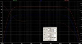
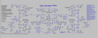
some sim results of the gain stage:
Pic 1: Amplitude response of the gain-stage.
A clean Bandpass response with bandwidth limits (F-3dB) at 0.75Hz and 1MHz. Vin and Vout(SE) are at 0dB, Vout(bal) at +6dB
Pic 2: Amplitude response of the gain-stage + Buffers.
A nearly identical clean Bandpass response with bandwidth limits (F-3dB) at 0.75Hz and 1MHz.
Vin and Vout(SE) are at 0dB, Vout(bal) at +6dB.
The output amplitude (magenta curve) at >1MHz rather shows the reactive behaviour of the output LR-network with the attached RC-load than the buffers behaviour.
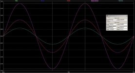
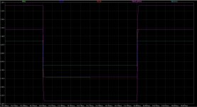
Pic 3: Transient response to a 1kHz 1Vrms in signal fed in balanced mode.
The curves for Vin (green),V1-2 (blue) and Vout(SE) (red) are overlapping and hardly distuingishable from each other.
The single Vnoninv input (light blue) is exactly -6dB lower and the balanced output (magenta) is +6dB higher.
It shows that the two trimpots in the gain-stage can precisely trim the gain to its desired value and to perfect interchannel balance.
Pic 4: Transient response to a 10kHz +-1.4142V in signal fed in balanced mode.
Colors are the same as in Pic 3.
One can see that the transient behaviour is almost fully defined by the input Bandpass´s transient response (blue).
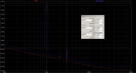
Pic 5: a FFT of a 1kHz 1Vrms in signal fed in balanced mode.
Vout(SE): 1Vrms
K2: 0.0002174% -113.2dB
K3: 0.0006776% -103.4dB all else insignificant.
THD(1-9): 0.000714% -102.9dB
Vout(bal): 2Vrms
K2: 0.0000670% -123.5dB
K3: 0.0006776% -103.4dB all else insignificant.
THD(1-9): 0.000684% -103.3dB
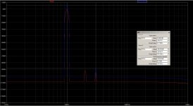
Pic 6: a FFT of a 10kHz 1Vrms in signal fed in balanced mode.
Vout(SE): 1Vrms
K2: 0.002777% -91.1dB
K3: 0.001565% -96.1dB all else insignificant.
THD(1-9): 0.003188% -89.9dB
Vout(bal): 2Vrms
K3: 0.001565% -96.1dB all else insignificant.
THD(1-9): 0.001565% -96.1dB
Now let´s hope, that the praxis confirms the simulations and that the gain-stage sounds equally well as the buffers.
jauu
Calvin
some sim results of the gain stage:
Pic 1: Amplitude response of the gain-stage.
A clean Bandpass response with bandwidth limits (F-3dB) at 0.75Hz and 1MHz. Vin and Vout(SE) are at 0dB, Vout(bal) at +6dB
Pic 2: Amplitude response of the gain-stage + Buffers.
A nearly identical clean Bandpass response with bandwidth limits (F-3dB) at 0.75Hz and 1MHz.
Vin and Vout(SE) are at 0dB, Vout(bal) at +6dB.
The output amplitude (magenta curve) at >1MHz rather shows the reactive behaviour of the output LR-network with the attached RC-load than the buffers behaviour.
Pic 3: Transient response to a 1kHz 1Vrms in signal fed in balanced mode.
The curves for Vin (green),V1-2 (blue) and Vout(SE) (red) are overlapping and hardly distuingishable from each other.
The single Vnoninv input (light blue) is exactly -6dB lower and the balanced output (magenta) is +6dB higher.
It shows that the two trimpots in the gain-stage can precisely trim the gain to its desired value and to perfect interchannel balance.
Pic 4: Transient response to a 10kHz +-1.4142V in signal fed in balanced mode.
Colors are the same as in Pic 3.
One can see that the transient behaviour is almost fully defined by the input Bandpass´s transient response (blue).
Pic 5: a FFT of a 1kHz 1Vrms in signal fed in balanced mode.
Vout(SE): 1Vrms
K2: 0.0002174% -113.2dB
K3: 0.0006776% -103.4dB all else insignificant.
THD(1-9): 0.000714% -102.9dB
Vout(bal): 2Vrms
K2: 0.0000670% -123.5dB
K3: 0.0006776% -103.4dB all else insignificant.
THD(1-9): 0.000684% -103.3dB
Pic 6: a FFT of a 10kHz 1Vrms in signal fed in balanced mode.
Vout(SE): 1Vrms
K2: 0.002777% -91.1dB
K3: 0.001565% -96.1dB all else insignificant.
THD(1-9): 0.003188% -89.9dB
Vout(bal): 2Vrms
K3: 0.001565% -96.1dB all else insignificant.
THD(1-9): 0.001565% -96.1dB
Now let´s hope, that the praxis confirms the simulations and that the gain-stage sounds equally well as the buffers.
jauu
Calvin
Attachments
-
 Differential-in-out hybrid CFP gain stage amp.jpg129.8 KB · Views: 1,109
 -
 Differential-in-out hybrid CFP gain-stage w hybrid CFP Buffer amp.jpg133.4 KB · Views: 907
 -
 Differential-in-out hybrid CFP gain-stage w hybrid CFP Buffer sine-1kHz.jpg69.4 KB · Views: 878
 -
 Differential-in-out hybrid CFP gain-stage w hybrid CFP Buffer rect-10kHz.jpg205.2 KB · Views: 893
 -
 Differential-in-out hybrid CFP gain-stage w hybrid CFP Buffer FFT-1kHz.jpg267.4 KB · Views: 200
 -
 Differential-in-out hybrid CFP gain-stage w hybrid CFP Buffer FFT-10kHz.jpg261.8 KB · Views: 209
Hi,
here´s the asc-file
Models:
LSK389Cco from Bob Cordell´s lib.
SST/MMBF4391 from ONSemi or Fairchild
BC847BS from Diodes/Zetex or NXP/Philips
FZT751/651 from Diodes/Zetex
Potentiometer from LTSpice Yahoo-group
jauu
Calvin
here´s the asc-file
Models:
LSK389Cco from Bob Cordell´s lib.
SST/MMBF4391 from ONSemi or Fairchild
BC847BS from Diodes/Zetex or NXP/Philips
FZT751/651 from Diodes/Zetex
Potentiometer from LTSpice Yahoo-group
jauu
Calvin
Attachments
Yes, pretty cool. Now we have a discrete preamp.
Just for fun i build the Piglets Dad Bootstrapped Diamond Buffer.
I do not post a schematic here, you can see it on the Pink Fish Media forum.
Dadod has shown something like that here and the Paradise 1 also had a diamond bootstrap buffer based on my idea and optimized by MiiB, although with a different principle.
Next post will show the performance.
Hi Joachim,
You can take a look at this pre/headphone amp. I think that is very cool with no GNFB and very low THD. http://www.diyaudio.com/forums/solid-state/235695-no-nfb-line-amp-gainwire-mk2-4.html#post3514957.
I made previous version of similar pre/headphone amp http://www.diyaudio.com/forums/anal...onveyor-voltage-amplifier-25.html#post3455500 and I am very satisfied with it, but this one uses less power and no exotic transistor(some JFETs no easy to find and there are lot of fakes) with similar level of THD and drive power.
BR Damir
Dadod, i am watching your work all the time but may have not told you.
I really like what you do.
I really like what you do.
Hi,
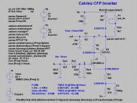
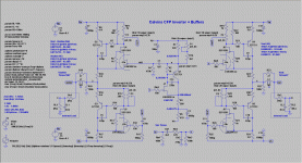
if someone doesn´t need or want the fully differential CFP gain-stage, he might just add an Inverter ahead of one of the Buffers.
Here´s an Inverter similar to the differential CFP gain stage as a CFP Inverter.
Again the JFET/bipolar CFP cell forms the heart of the circuit.
Basically I omitted with the tail current source and cut the differential stage in half. Most anything left remained the same.
In the final circuit with Buffers a compensation cap C14 needed to be added from the bipolars base to its collector.
It should be obvious, that the behaviour the two branches -Buffer alone vers. Inverter + Buffer- is not precisely the same.
This could be regarded as a disadvantage against the fully differential circuit, as well as only gains of +1 and -1 are feasa
ble.
jauu
Calvin
Attachments
Hallo,
I am thinking about making a self-etch-PCB for the buffer in post 87 (left side), and I have a question about the choice of transistors.
The used LSK389 is a dual jfet. Is it important to to use them in a dual package, because there is also a single-fet version available (the lsk170)? I assume this is due to thermal coupling of the V+ and V- transitor, isn´t it?
An alternative would be to use the 2SK369 that joachim did. They seem to be a drop in replacement...
Thanks
Flo
The 2sk369 is a single device. Same legs as the k170.
The 389package has the two sets of 3legs in line with a dummy in between.
That prevents (easy) gluing two single devices together for better thermal coupling.
The 389package has the two sets of 3legs in line with a dummy in between.
That prevents (easy) gluing two single devices together for better thermal coupling.
Hi,
the protos seem have been running well without thermal coupling, but I´d recommend it with this kind of circuit. The 2SK170/LSK170 came in TO92 casing which can easily be put/glued together thermally. With the 2SK389 and LSK389 there´s already a single casing. I personally prefer the SOIC8 of the LSK389 (besides beeing an active part whereas the 2SK389 is obsolete).
The SOT23 casing in which the 4391 come built a bit less high and may be placed in close proximity to the LSK389. The three may then be thermally coupled by one cooling fin for DIP-casings or power-LEDs. The SOT223 Zetex FZT751 may have their own copper areas with associated cooling fins.
With the TO92 LSK170 it´d be logical to use 2N4391 as cascodes, as those come in TO92 too. I´d place the 4 transistors in a small square array and glued them to a T-type cooling fin.The FZTs could then be replaced by suitable throughhole types in TO126 or TO220 casings and dedicated cooling fin each.
jauu
Calvin
I would suspect that the most important issue to thermally mange is the input stage, as the buffers have a gain of one, there should be no difference there, off course there could be a thermal drift of the output offset.
Thanks for the help, very appreciated.
I guess thermal coupling can be done very easily, either with soic or to92 packages.
Maybe I´ll do a layout for both, I will see.
The choice of FETs also seems to be a question of availability:
LSK389 and LSK170 are available from trendsetter-electronics in different packages.
I assume the ZTX751 is the to92 version of the FZT751, they are both readily available everywhere and I think I still have some of the ZTX751.
pn4391 or 2n4391 are easy to find, unlike the sst4391 in SMD package... (at least I did not find them).
So I guess I´ll start with a to92 layout.
- Home
- Source & Line
- Analog Line Level
- Preamp-Buffers - simple idea