So, I've had a quad paralleled TDA1387 from Tek Products laying around for a few years now waiting for a project and I recently had some renewed interest in doing something with it. After a couple of false starts I've arrived at this configuration - NOS with passive I/V and LP filter followed by a current source loaded cathode follower at the output.
Attachments
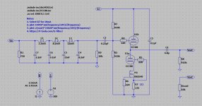
I've modified the TDA1387 board to remove the onboard I/V network and coupling capacitors. The DAC output is now directly coupled to I/V resistors which are located on a separate LP filter board.
The I/V resistor is 750 ohms, which provides the input impedance to a 7th order passive LP filter whose values have been adjusted to compensate for the sinc droop at the DAC output. With the 750R I/V resistor, output is around 0dBv at full output.
The I/V resistor is 750 ohms, which provides the input impedance to a 7th order passive LP filter whose values have been adjusted to compensate for the sinc droop at the DAC output. With the 750R I/V resistor, output is around 0dBv at full output.
Nice simple circuit. Aside from the 7th order passive reconstruction filter, of course. I'm a big fan of passive resistor I/V where the DAC has enough low distortion output voltage compliance. I also like the tube cascode of the M1 current source.
Thanks. I've also done this with a 3rd order filter. Others (Abraxalito) feel that a higher order filter improves the sound somewhat. I can't say that I've noticed much of a difference between the two. Compensating for the sinc droop, though, makes a big difference, IMO.
Marcus, with your NOS DAC experience, I'd like to invite you to participate in our thread (link below) which is investigating why OS and NOS DACs sound characteristically different, when it seems they should not. We have a list of suspected technical causes, and are working our way through it. Our goal/hope is to identify a DAC architecture/design 'formula' which combines the best of OS sound with the best of NOS sound.
What do you think makes NOS sound different?
What do you think makes NOS sound different?
I've also done this with a 3rd order filter. Others (Abraxalito) feel that a higher order filter improves the sound somewhat. I can't say that I've noticed much of a difference between the two.
The 7th order filter I'm using has a considerably steeper transition band than the one you're showing in post #1. That might make a difference.
How did you incorporate the NOS droop compensation into the basic design (which I assume you adopted from rf-tools as you mention them)? I haven't found a mathematical way to do that, I just play around in LTSpice - I'm curious if there are more formal methods to achieve the same.
Anyway great to see more applications of TDA1387 and LC filters 🙂
Ken,
I've been lurking on that thread. I'm interested to see where tat goes, though I don't feel like I'm in a position to contribute at the moment.
Abraxalito,
I'm unaware of any formal methods to do the droop compensation. I'm also just manually adjusting component values in LTspice. Filter improvements are among the items I'll be looking into as I move forward.
Marcus,
How would you describe the subjective performance of the output buffer shown in your schematic, as compared to other buffers which you may have tried?
How would you describe the subjective performance of the output buffer shown in your schematic, as compared to other buffers which you may have tried?
Of the buffers I've considered, this one is the least colored by far. Compared with them it has good detail and a good sense of space. The midrange is nice and the bass is solid. It seems to mostly just get out of the way. My goal was a good sounding tube buffer that can drive a 10 kohm load and I'm pretty happy with the result so far. I do feel the shunt regulator is an important part of the buffer's sound.
Other configurations I've considered include a Broskie ACF and SRPP circuits. Ultimately I rejected them in favor of this one.
Other configurations I've considered include a Broskie ACF and SRPP circuits. Ultimately I rejected them in favor of this one.
After living with this for a while now I've developed a clear preference for the 3 pole reconstruction filter of the 7 pole version. The 3 pole filter seems to produce a better high frequency balance, where the 7 pole seems recessed or a little rolled off. It's not clear to me why. They do both have a few tenths of a dB deviation from flat response in simulation, but I don't really see a correlation between that and the perceived sound.
Another difference is that the 3 pole uses a smaller I/V resistor (560R vs 750 for the 7 pole), so maybe the TDA1387 is happier with the smaller value.
Another difference is that the 3 pole uses a smaller I/V resistor (560R vs 750 for the 7 pole), so maybe the TDA1387 is happier with the smaller value.
Attachments

Marcus,
What kind of filter inductor cores are in use? Air core? Ferrite?
What kind of filter cap construction?
Maybe factors other than frequency and or phase response have some effect your preference for a simpler filter?
What kind of filter inductor cores are in use? Air core? Ferrite?
What kind of filter cap construction?
Maybe factors other than frequency and or phase response have some effect your preference for a simpler filter?
Last edited:
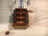
That's an interesting point. The inductors are Bourns RL181S series, so definitely ferrite core. The capacitors are Panasonic ECWH polypropylene film.
Phase response by simulation is -55 degrees for the 3 pole and -240 for the 7 pole at 20 kHz, no surprises there.
Phase response by simulation is -55 degrees for the 3 pole and -240 for the 7 pole at 20 kHz, no surprises there.
Attachments
I'm curious about your result with the two filters - there could be something in the resistor value difference.
As the TDA1387 has unipolar current output there is a static current (almost 600uA) coming out at digital zero. This current has noise (at the very least in an ideal current source it has shot noise and we can assume its less than ideal) which gets turned into voltage by the I/V resistor. So there's a noise source effectively in series with the I/V resistor when its biassed with a static current. If the static current is 'bled' away with an external CCS then that noise source can be eliminated.
As the TDA1387 has unipolar current output there is a static current (almost 600uA) coming out at digital zero. This current has noise (at the very least in an ideal current source it has shot noise and we can assume its less than ideal) which gets turned into voltage by the I/V resistor. So there's a noise source effectively in series with the I/V resistor when its biassed with a static current. If the static current is 'bled' away with an external CCS then that noise source can be eliminated.
Thanks. I've also done this with a 3rd order filter. Others (Abraxalito) feel that a higher order filter improves the sound somewhat. I can't say that I've noticed much of a difference between the two. Compensating for the sinc droop, though, makes a big difference, IMO.
Hi,
Did you notice a difference with no input filter at all ?
Noob question : why not a single ECC88 with each triode stage for one channel instead ? Not enough current from the TDA1387 VS a TDA1541A (4 ma ptp) for illustration ?
thanks for the shematic, not enough seen those days...
Last edited:
Abraxalito,
That's an interesting conjecture and solution that I hadn't thought of. I have some reservations about implementing it. Unless I'm misunderstanding your description, it seems like such a configuration would pull the TDA's output pins to near ground potential and that they would then be driven negative for a part of the cycle during operation. I wonder what effect that might have on chip operation. It seems like a clear violation of the compliance range at the very least.
That's an interesting conjecture and solution that I hadn't thought of. I have some reservations about implementing it. Unless I'm misunderstanding your description, it seems like such a configuration would pull the TDA's output pins to near ground potential and that they would then be driven negative for a part of the cycle during operation. I wonder what effect that might have on chip operation. It seems like a clear violation of the compliance range at the very least.
By no means is it necessary to violate the compliance range of the DAC. One way to implement it would be to create a low noise reference voltage at roughly half the compliance range (say +1.75V) and connect the I/V resistor between this reference and the DAC's output. Then a suitably sized current source (~600uA per chip) between the DAC's output and 0V makes the resultant current into the I/V resistor bipolar.
diyiggy,
The lower triode section and the FET together form a cascoded current source with quite high impedance. It's usually accomplished with 2 FETs, I just liked the idea of using a triode in that location. It's supposed to be a tube buffer, after all.
Yes, I have tried this with no filter at all and the sinc droop is very noticeable. I'm currently using a 3 pole filter which attempts to compensate for the sinc droop. It's not particularly effective as a reconstruction filter, although it will knock down some of the higher frequency images.
Personally, I find the sinc droop compensation a necessity.
By no means is it necessary to violate the compliance range of the DAC. One way to implement it would be to create a low noise reference voltage at roughly half the compliance range (say +1.75V) and connect the I/V resistor between this reference and the DAC's output. Then a suitably sized current source (~600uA per chip) between the DAC's output and 0V makes the resultant current into the I/V resistor bipolar.
Ah, I see that.
- Home
- Source & Line
- Digital Line Level
- Yet another TDA1387 NOS DAC with tube output