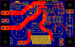
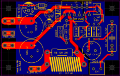
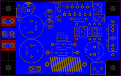
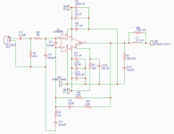
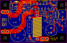
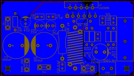
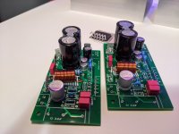
I like the design, heavy current stuff away from the signal area, well thought out.
Only comment is that the ground plane seems to extend also on the signal area.
I would not do that, you have no control over where currents flow in a ground plane, and it could inject junk into the signal area.
If you want to use ground planes, separate the power supply area and the signal area in two planes, interconnected at a single defined point where no current flows.
Or forget about a ground plane in the power supply area, it won't do anything for the sound anyway, and rely on the heavy tracking.
BTW I think you miss a hole for pin 2 of the amp.
Jan

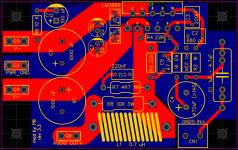
BTW I think you miss a hole for pin 2 of the amp.
I'm just going to clip it off - it is not used anyways. I am using that space on PCB to route V- trace of at least 5mm width - rated to 2.5A I think...
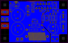
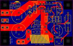
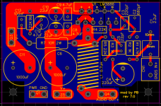
Rev 3.2.2
- updated 1W and 3W resistor sizes
- input now has 5mm connection terminal
- doubled traces for V-, V+
- updated 1W and 3W resistor sizes
- input now has 5mm connection terminal
- doubled traces for V-, V+
Attachments
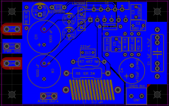
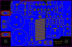
Rev 4.0:
- zener diode is gone now
- thicker routes for V+ V- and SPK out
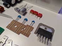
- LM3886 legs #2 and #4 are connected
Attachments
Last edited:
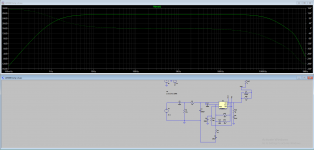
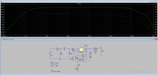
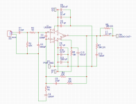
I was able to finally load LM3886 model into the LTSpice simulator. Now, based on that, I have came out with adjusted schematics.
Input capacitor C1 and resistor R1 are 2.2uF and 47K respectively. Cutoff freq = 1.54 Hz
Feedback capacitor C4 = 220uF. You can improve a little by upgrading to 330uF, but the difference is very very small, and starts from 10Hz and lower. Mostly improvement is in the phase by 5 degrees and 0.2dB less rolloff to the low end of 10Hz.
High pass R2 =1k and C2 = 1000pF => Cutoff freq = 159kHz.
C3 is value from the datasheet and is 220pF.
C5 makes rolloff after 150kHz steeper in angle. 15pF is very safe value. Can be increased to 27pF, 33pF, but I would not recommend values higher than that.
C13 makes the whole HF to roll off steeper, especially closer to 1MHz. Can be increased to 0.22uF without any issues.
Attachments
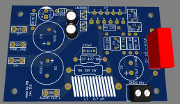
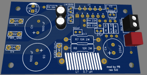
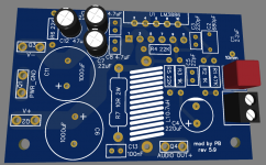
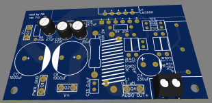
Rev 5.0
New size - 45mm by 80mm. Used X7R and C0G for all capacitors, except input low and hi pass filters.
New size - 45mm by 80mm. Used X7R and C0G for all capacitors, except input low and hi pass filters.
Attachments
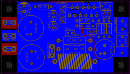
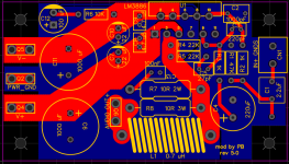
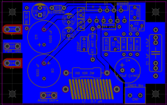
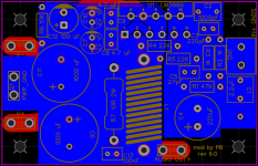
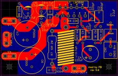
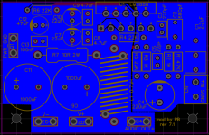
Rev 6.0
PCB size is reduced to 45mm by 70mm
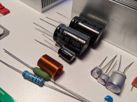
Inductor L1 and output resistor R8 are made of wire wrapped around the resistor and take space for only one part
V- and V+ are 5mm traces
Out pin #3 trace is 5mm to the L1 and further down
Parts list updated
PCB size is reduced to 45mm by 70mm
Inductor L1 and output resistor R8 are made of wire wrapped around the resistor and take space for only one part
V- and V+ are 5mm traces
Out pin #3 trace is 5mm to the L1 and further down
Parts list updated
Attachments
Thank you!Nice progress, nice board! 🙂
I noticed you got rid of the zener too - it just didnt work for me.
Iv'e read forums and found people were having issues with those zener diodes. Also, datasheet doesn't have it, so I don't think it is that important. 100uf +10k cap and resistor give 1 sec delay so I'm good with that.

Layout works only with certain location for LM3886 pins. V+ and V- is on the left, so is main out. All inputs are on the right. To mirror the layout, you will need a chip that has pins mirrored, otherwise you need to cross bunch of traces.Would it be possible to design a mirror board? Left and Right board?
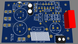
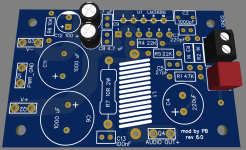
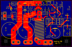
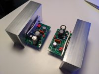
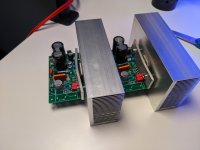
I ended up redesigning layout one more time - this time is because I used aluminum bar to mount LM3886 chip to the heatsink. The bar got in the way of many components located closer to the heatsink. That was fixed in this revision.
This revision also has minor fixes based on my soldering experience - improved components locations and increased soldering pads where needed.
This revision also has minor fixes based on my soldering experience - improved components locations and increased soldering pads where needed.
Attachments
Last edited:
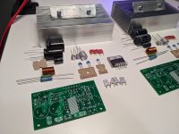
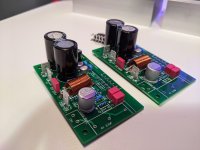
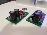
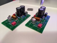
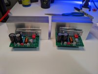
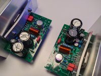
Finally got around to put two channels together.
Attachments
-
 PXL_20220413_000415709.jpg421.4 KB · Views: 128
 -
 PXL_20220413_000437393.jpg325.3 KB · Views: 107
 -
 PXL_20220413_000442679.jpg344 KB · Views: 105
 -
 PXL_20220413_021819998.jpg322.9 KB · Views: 105
 -
 PXL_20220413_021805854.jpg300.4 KB · Views: 105
 -
 PXL_20220413_021731376.jpg269 KB · Views: 113
 -
 PXL_20220413_021657894.jpg297.1 KB · Views: 122
 -
 PXL_20220413_032049542.jpg359.1 KB · Views: 128
 -
 PXL_20220413_032001208.jpg272.4 KB · Views: 115
 -
 PXL_20220413_031944335.jpg270.8 KB · Views: 116
 -
 PXL_20220413_032039283.jpg414.6 KB · Views: 127
- Home
- Amplifiers
- Chip Amps
- Yet another LM3886 gainclone PCB based on circuitbasics.com