Got the new Control Boards back yesterday. I'll build this up over the weekend, and report back.
The boards at 2X cost $70 each (incl. tax and postage). They are much cheaper in quantity, but you have to buy a couple to determine if they work in the first place. So, assuming this one works properly, I'll sell it to you at my cost, which will be $70 plus postage - probably about $75.
Scott
Keep me posted on this Scott- if successful I will take the second board. (will help a bit with your prototyping costs!)
Update.
Stuffing the new board. About 70% complete.
Only issue I have found is that the holes for the heatsinks are mis-positioned slightly, so the heatsink sits about 1/16 inch back from the leads on the transistor. I could bend the leads, but then the heatsink interferes with the 5/11 and 6/10 lead connections.
So, I removed the pins from the heatsinks, and just have them held in place by the transistors themselves. Seems to work OK, and it puts the heatsinks in the right position. The amp isn't going to be under a lot of heavy vibration... so it should be durable that way.
I need to inventory my transistors, and capacitors. If I have everything, I should be ready to fire this up tomorrow.
Cheers,
Scott
Last edited:
Hi Scott,
Here is hoping for a complete success with your new PCB.
-Chris
Oops! Oh well.the holes for the heatsinks are mis-positioned slightly, so the heatsink sits about 1/16 inch back from the leads on the transistor. I could bend the leads, but then the heatsink interferes with the 5/11 and 6/10 lead connections.
Here is hoping for a complete success with your new PCB.
-Chris
Board stuffing is proceeding. Had to stop to get diodes and a couple of transistors.
I checked out the BOM for the board, and I can't see how it could be realistic to fab these complete.
The total for all new parts KOA Speer film resistors, WIMA caps, and semiconductors totals out at $160. Add to that a board for $75 in low quantity, and the basic cost for a completed board is $235. And that's not including any profit or labor for stuffing and checking the board. This assumes NTE and other equivalents for the non-signal path devices (the bias diodes and the 2SA970/2SC2240 devices), and LittleDiode NOS parts of the signal path parts. That totals out to $110 plus shipping from the UK.
To make that worth the time, I'd have to sell completed boards for about $300.
So, I think I may do some runs of the boards, and either sell them blank, or sell a kit of caps and resistors, and let the users swap over the heat sinks and parts from their existing board.
Scott
Got the transistor matcher boards today. I am off for the labor day weekend, but will build that up and match the Darlingtons for the new control board early next week.
I also received my copy of Bob Cordell's book on amplifier design. He makes a good point that not only do the diff pairs need to be matched, but you should also try to match the NPN and PNP pair betas.
I'll see how realistic that is in practice. The core problem will be that the beta of a Darlington is about 10K, so I expect quite a lot of beta variation between them.
S
Hi Scott,
Yes, complimentary diff pairs must be matched as well. It is important and does lower distortion. I've also been saying that for years.
When you have all four transistors matched, guess what happens? The net DC base current drops to very nearly zero. This is good news for DC offset reduction. I'm not sure how this would work, but I suspect that the positive and negative swings of the input signal now have equal impedance to work into. Unfortunately, the PNP pair probably have higher capacitance. That's something I would have to look up. It can be experimented with by sending a high impedance input signal into various input stages to see which has the lowest "pre-distortion". This may, or may nor, explain my own personal preference for J-FET input stages.
-Chris
Hi Scott,
Yes, complimentary diff pairs must be matched as well. It is important and does lower distortion. I've also been saying that for years.
When you have all four transistors matched, guess what happens? The net DC base current drops to very nearly zero. This is good news for DC offset reduction. I'm not sure how this would work, but I suspect that the positive and negative swings of the input signal now have equal impedance to work into. Unfortunately, the PNP pair probably have higher capacitance. That's something I would have to look up. It can be experimented with by sending a high impedance input signal into various input stages to see which has the lowest "pre-distortion". This may, or may nor, explain my own personal preference for J-FET input stages.
-Chris
Yeah, Cordell, specifically points out that this issue is not found in JFET input stages. OTOH, JFETS are generally noisier...
Hi Scott,
-Chris
I have not found this in practice. On the bench, compared to the same amplifier - maybe. In practical terms I wouldn't worry about it. Your room background noise will completely swamp amplifier noise unless you are using some really efficiency horn speakers.JFETS are generally noisier...
-Chris
Hi Scott,
I have not found this in practice. On the bench, compared to the same amplifier - maybe. In practical terms I wouldn't worry about it. Your room background noise will completely swamp amplifier noise unless you are using some really efficiency horn speakers.
-Chris
Yeah, it might not be an issue for practical purposes. The issue with FETs is simply that the gate-source junction is effectively a capacitor, and any noise voltages (i.e low energy noise that has little current associated with it...like background radiation) gets amplified along with the signal. I am sure better gate design and smaller gates have gone a long way to resolve this. Back in the mid 80's I managed a project where we made the world's lowest noise microwave amplifier (1.5 dB NF at 12 GHz). For that we used an electron beam lithography setup and made a 0.7 micron T-shaped gate (so there was more metal in the gate, but no more capacitance at the junction). It cost millions, but worked great!
Cordell's book is very interesting!
Scott
Hi Scott,
Yes, I have read Bob's book, and also Doug Self's books. I keep them as reference material. They are both highly recommended to have. Lot's of great information in each.
As you know, BJTs aren't free from capacitance, and it can be non-linear too. As for the noise, you aren't working on an LNA, so the little extra noise (from lower transconductance than BJTs) doesn't even come up. In some situations (source Z > 1K0) they can perform better than BJTs.
Let me know how the balancer / matcher works out for you ...
-Chris


I am also mostly done with Version II of the 565 control board. I need to match some Darlingtons for it, and then it will be ready for some juice.
I'll keep you folks posted.

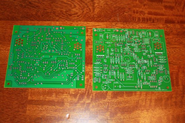
The sharp eye will note that C108 is "missing". It is actually on the back side in this iteration. The WIMA caps were a little fatter than I expected. I fixed this is in Version III.
I'll keep you folks posted.
The sharp eye will note that C108 is "missing". It is actually on the back side in this iteration. The WIMA caps were a little fatter than I expected. I fixed this is in Version III.
Hi Scott,
That's a really nice board for both. You have a talent that I don't.
As for some components on the back of a PCB, I have done that from time to time to keep heat sensitive parts away from another hot component, or from rising heat. The rear of a PCB can be very useful for this type of thing. It's also a nice place for axial capacitors that are too large to lay out. Look how much room you gain by putting those on the rear of a PCB.
Let us know how they both work out. One question for you. Did you insulate the LED from ambient conditions with some foam, or not?
Best, Chris
So far I have not insulated the LED or the transistor. Try as I might, I could not find an LED that actually fit in the TO126 hole. So the LED sits above the transistor, and I use a plastic cover over the board It seems to stabilize after about 30 seconds (much faster than my old breadboard setup!)
The only thing I would change is to put a ground test point lug on the board, and to label the test points so you know what they are in terms of the circuit (NTP1A isn't very informative...)
I am measuring about 0.2 micro amps of base current( 0.2 mV over 10K ohms), and about 1.25 mA of collector current, which computes out to a beta for the Darlington of about 60K..Does this seem right? That's a beta of about 250 for each junction, so it seems reasonable...
Board seems pretty stable and easy to use (other than the lack of a ground test point)> I'd suggest we include an Excel file with a test data sheet that computes offsets and overall match, as well as beta, and include some instructions for what data to take at what test points (basically a little procedure and a data sheet). To address potential offsets in the test board, I test the transistors using a matrix that ends up with each transistor in either position, so you test them one way, and test them the other way. The difference in the measurements then gets averaged out so you can back out any residual offset from the test jig. 2x the measurements, but 10X the accuracy.
I'll post the gerber files after I update the board.
Chris, if you want a copy of either or both of these boards PM me your address. After all the help you have provided, it is the least I can do in payback..
Scott
Last edited:
Hi Scott,
The important thing is to tightly match the collector / Drain resistors and the base / gate resistors. I bought 0.1% resistors for those positions. The position of the transistor can't make any difference when you do it that way. Simplify your life if you didn't get that close in those resistors. The gain of the Darlington transistors don't matter at all. It's only important to balance the two in the jig, so hang your meter across the two 100 R resistors on the DUT sides. You want the lowest reading on the meter.
A 3mm red LED will fit in those holes just fine. The lower skirt will keep the diode from coming out as you solder it in. The pass transistor will sit off the board high enough for some closed cell foam in there. I used some pink foam that some parts are shipped in. Don't use the black stuff. I suspect that some kinds are slightly conductive and may disintegrate over some time.
If the 3mm LED won't fit in, file or sand the sides slightly so it fits snuggly. A little thermal compound will help the heat transfer. I forgot about that step. I used a drill press and a small modelers file to reduce the diameter of the LED. Just have a TO-126 transistor to fit the hole as you go. We want the transistor to heat the LED and there is a lot of heat loss through the LED leads. Also, the leads have projections so the LED will not go through the board all the way. This works for us in this case because a longer lead reduces heat loss that way.
For the sockets, use parts sold at Digikey, Mouser or Newark. The ones from China are terrible in that the leads don't fit well. They catch on the upper lip. Avoid. The capacitors exist to keep any DUTs from oscillating. The values are not critical. The resistors that set tail current don't have to be exact either. What works on one may not be right on another. The differences between pass transistors and LED voltage drops will direct affect the actual tail current. So don't fret if the values aren't bang on, and do feel free to change the values to suit. The only real desirable characteristic for the resistors is that they have a low temperature tempco. 50 ~ 100 ppm would be preferred. All you should care about is that the current is stable and somewhat close to the value they will be running at.
Hey Scott, that's a generous offer. I'll take you up on that so I can test it. It might even replace the one I'm using!
The tip of the 3 mm LED fits, but the body doesn't.
I ended up putting the transistors down, and then put the LEDs on top of them, holding them down to the board. That way the heat from the transistor will rise to the LED. I used a copper ground plane on the board, so it is all pretty thermally stable. I would think thermally insulating the devices would cause ether to drift independently, whereas making them all thermally connected would assure that everything drifts together.
I measured my resistors They are within 0.1%. This "should" result in an offset of less than 0.2 mV. However, I also tested two transistors in the two positions. In one position the collector voltage difference is -7.4 mV, and wight he devices swapped, it is +5.5 mV. This indicates that the actual match is very close.
To understand this we can make the following statements. We are seeking the collector differential voltage in a perfectly balanced jig. Let's call this Vc. We can call the differential voltage measured at the test points Vm, and we can assume that the circuit has an unknown fixed offset between the two legs at the current level being tested. Call this Vo. Now since we know that the collector differential voltage Vc will change polarity depending on which side of the jig each transistors is in. Put them in one way and you might measure, for example -7.4 mV, swap positions, and you measure 5.5 mV (these are actual numbers from my tests).
Now the fixed offset Vo of the jig doesn't change when we swap transistors around..So we can write out the following relations:
Vm1=Vo+Vc
VM2=Vo-Vc
Where Vm1 and Vm2 are the two different measurements taken wight he transistors in one position and the other.
We can, of course subtract these equations, and thereby eliminate the offset entirely. So we get:
Vm1-Vm2=2Vc, or Vc=1/2(Vm1-Vm2)
Using my numbers above, I get (5.5-(-7.4))/2=6.45 mV This is the actual collector match.
Knowing this, you can also go back and compute the jig offset, which in this case is 0.95mV
So, technically, having done this once, I suppose you could then just do the measurements on way, and correct them by 0.95 mV
Interestingly, I tried simply shorting the emitter and collector points and measuring the offset, and for 0.8 mV.. so I think this is a pretty accurate approach.
Hi Scott,
Now work out your error budget. You may find that you are well withing experimental error.
If your resistors are within 0.1% of each other, then your matches will be insanely close with those readings. Even imperfect matches (but close) will demand that you match any emitter degeneration resistors in the actual circuit or they will actually through your match off. Like I said earlier, don't worry about figuring out the gain, just balance the transistors. With darlington transistors, beta values aren't that important (they are really high), but you can balance them with the jig. You're getting right to the meat of the matter.
-Chris
I find that the jig offsets seem to depend a bit on the transistor. They vary by about +/-1.5 mV. Weird. Must be some impedance interaction..so by measuring them both ways in the jig, I can be certain that the offset for that transistor is computed out.
So for example, I am matching 25 devices (yeah 600 measurements.. ugh)..
I measured -2.4 mV offset with the device in one position, and -0.2 mV in the other. The net offset is thus actually 1.1 mV (A pretty good match!). this is basically just an averaging approach, and it nulls out not only the offset, but any drifty caused by not letting the devices cook long enough.
I have also noticed that some devices settle down in a matter of a 5-10 seconds, while other just drift along for 30-60 seconds..
- Home
- Amplifiers
- Solid State
- Yet Another Adcom GFA-565 Thread